DON´T build this one!
I just encounterd a huge error, tho another gate driver may fix it.
I also suggest you using the LT1016 comparator that titanchen used in his amp.
I just encounterd a huge error, tho another gate driver may fix it.
I also suggest you using the LT1016 comparator that titanchen used in his amp.
hey tekko
have drawn the schematic in the eagle and was working further
BTW what happened.IR gave up?
how about HIP4080?
Sagar
have drawn the schematic in the eagle and was working further
BTW what happened.IR gave up?
how about HIP4080?
Sagar
HIP4080 is a good one, but made for fullbridge, not halfbridge.
I suggest you get IR2010/2110/2113 if you want to make a halfbridge amp.
IR2111 has too long deadtime, 650nS causing tremendous distortion and only allows for a third of the rail voltage in output.
I suggest you get IR2010/2110/2113 if you want to make a halfbridge amp.
IR2111 has too long deadtime, 650nS causing tremendous distortion and only allows for a third of the rail voltage in output.
ok
you say your amp has problem bec of drivers.
so replacing with a suitable IR will solve the problem?
Sagar
you say your amp has problem bec of drivers.
so replacing with a suitable IR will solve the problem?
Sagar
Hi Tekko🙂
I'm home🙂. I noticed your schemo has an error on it b'coz the fet driver must be triggered via pin 2 with respect to pin 3 "Gnode" as ground. The problem with the schemo is that the signal source has a split supply having a +/- 5V whose output is referenced to center tap neutral . This means that your signal is nowhere to go
The best remedy is to change the overall biasing schemes using single ended supply so that all signals are referenced to digital ground "Gnode" and then only the speaker is referenced to CT neutral.
Regards
ledmania
I'm home🙂. I noticed your schemo has an error on it b'coz the fet driver must be triggered via pin 2 with respect to pin 3 "Gnode" as ground. The problem with the schemo is that the signal source has a split supply having a +/- 5V whose output is referenced to center tap neutral
. This means that your signal is nowhere to go The best remedy is to change the overall biasing schemes using single ended supply so that all signals are referenced to digital ground "Gnode" and then only the speaker is referenced to CT neutral.
Regards
ledmania
Tekko, dont mind the level shifter. It is just there for level shifting of signal to a higher level and has nothing to do with the digital global ground inputs.... Just contemplate😉
Hurray! Let's confuse him! 
There is absolutely no problem with signal levels. Emitter current is alternating between 0 and 1,9 mA, therefore Uin is 0 and 12,9V relative to pin3. It should be a little less.
There is absolutely no problem with signal levels. Emitter current is alternating between 0 and 1,9 mA, therefore Uin is 0 and 12,9V relative to pin3. It should be a little less.
leddie, i suggest u look @ titanchen´s schemo in the post filter feedback thread.
Pafi, your not funny
Pafi, your not funny
Pafi said:Hurray! Let's confuse him!
There is absolutely no problem with signal levels. Emitter current is alternating between 0 and 1,9 mA, therefore Uin is 0 and 12,9V relative to pin3. It should be a little less.
I'm sorry Pafi, I dont want to confuse Tekko but based on my analysis thru his schemo, the output of the TLC393 is +/- 5Vac relative to "neutral" (neglecting losses) then rectified by D1 to convert to pulsed DC. Therefor the input to pin 2 is very much less than 10 if referenced to pin 3 but less than 5V relative to neutral.
I noticed also that Q1 has no level of amplification, no current gain because it is not triggered via the base(which is referenced to neutral again). Something is mixed up
.Lets say if D1 conducts to logic 1, Q1 is triggered giving Less than 5V relative to neutral, but when change to logic 0, D1 has no "sink"capability so the pulldown is initiated by the collector resistor which is referenced to Gnode..A mixed of referenced signal
.
I talked about the latest, the one which shows R1=1k, R6=1k, R9=6,8k.
Input voltage to neutral is irrelevant, and depends on supply voltage very much.
"no level of amplification, no current gain"
No current gain, but there is voltage gain because of the high load impedance!
Calculate! Emitter current at high output of comparator: (5V-0,6V-0,6V)/2k=1,9mA. Collector current is approx. equal to emitter current, so 1,9 mA flows trough R9. 6,8k*1,9mA=13 V. At low output emitter current is 0.
sagarverma said:why dont you post the proposed corrections?
Sagar
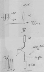
Can you try for these? At least this has a compatible interface to the input of the fet driver..Everything is in reference to Gnode...This will eliminate the faint beep that Tekko is keep of complaining. I think this will also reduce clipping @ 6 to 7V output from the fets....
An externally hosted image should be here but it was not working when we last tested it.
Pafi said:I talked about the latest, the one which shows R1=1k, R6=1k, R9=6,8k.
Calculate! Emitter current at high output of comparator: (5V-0,6V-0,6V)/2k=1,9mA. Collector current is approx. equal to emitter current, so 1,9 mA flows trough R9. 6,8k*1,9mA=13 V. At low output emitter current is 0.
Pafi, Lets try this...At logic 1, the total current across R1,R6,R9=.0004318..this is based on your 5V-.6-.6=3.8V. therefor the voltage that will appear across the 6.8kR is 0.0004318x6.8k=2.93V
This voltage is not enough to fire the fet driver into full swing🙂
Yes Pafi is right, the levelshifter does work.
It's a common basis circuit to make it fast enough.
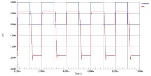
I tried simulating it (did you do that Tekko???) and it seems thet maybe the resistor R9 is a bit too large, and that the input level into pin 2 is somewhat more than 12 V with reference to -19V which is the ground level for the IR2111 (pin 3).
Try lowering the value to 4.7k or 3.3k, it should make the wavefom better as well.
Tekko have you measured the input to the level shifter, making sure it runs between +/- 5V (see my draving test point 1) with regards to gnd for your modulator???
Try also measuring the input to IR2111 between pin 3 and 2 to make sure it swings 12 V (not too much more and not too much less).
If all this works then proceed in changing the driver to a type with less delay.
It's a common basis circuit to make it fast enough.
I tried simulating it (did you do that Tekko???) and it seems thet maybe the resistor R9 is a bit too large, and that the input level into pin 2 is somewhat more than 12 V with reference to -19V which is the ground level for the IR2111 (pin 3).
Try lowering the value to 4.7k or 3.3k, it should make the wavefom better as well.
Tekko have you measured the input to the level shifter, making sure it runs between +/- 5V (see my draving test point 1) with regards to gnd for your modulator???
Try also measuring the input to IR2111 between pin 3 and 2 to make sure it swings 12 V (not too much more and not too much less).
If all this works then proceed in changing the driver to a type with less delay.
Attachments
- Status
- Not open for further replies.
- Home
- Amplifiers
- Class D
- SFX Class D subwoofer amplifier modification