I would definitely ground the RF cap to case, not signal ground. Don't want to inject it into anything directly connected to sig ref.
You can buy Neutrik XLR connectors with a build-in ring of RF caps to the shell.
You can buy Neutrik XLR connectors with a build-in ring of RF caps to the shell.
Ok so I was thinking correctly regarding C1 and C2. 🙂 I'm unclear whether that can be extended to R3-6.
I've seen the EMC series Neutrik connectors and have used the EMC cable connectors, but the EMC chassis connector is an ugly looking thing.
I've seen the EMC series Neutrik connectors and have used the EMC cable connectors, but the EMC chassis connector is an ugly looking thing.
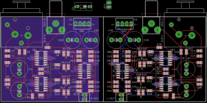
Latest with GND planes drawn for right channel. You can see why I left them off before. There's about 75mil or more gap between components/planes and the v-score mark through the centre of the board. I'll decide at a later point whether to ask the board house to do the v-score (I've never requested this before).
On the grounding of R3-6 (schematic in post 1) I'm inclined to switch them to circuit ground leaving C1 / C2 grounded to the XLR/chassis.
Re the jumper to open circuit the RCA connection when balanced connections are used, I was originally thinking of a two pin jumper but then it occurred to me that the header pins would be like an antenna connected to the circuit when the jumper is removed for balanced input use. Incorrect thinking? Perhaps a single position dip switch would be better...or perhaps it is completely unnecessary.
Still unsure re Jan's comment regarding grounding the unused connection to the unity gain buffers when SE connections are used. I will take a look at Self's discussion again but it seems to me that Fig 18.10 and the related text suggest that grounding the input isn't necessary...but I am the novice 😱
That's what I was thinking. Given the LME49740 is end of life perhaps others would offer their view as to whether the LMP8674 represents a likely/probable drop-in replacement.
On the grounding of R3-6 (schematic in post 1) I'm inclined to switch them to circuit ground leaving C1 / C2 grounded to the XLR/chassis.
Re the jumper to open circuit the RCA connection when balanced connections are used, I was originally thinking of a two pin jumper but then it occurred to me that the header pins would be like an antenna connected to the circuit when the jumper is removed for balanced input use. Incorrect thinking? Perhaps a single position dip switch would be better...or perhaps it is completely unnecessary.
Still unsure re Jan's comment regarding grounding the unused connection to the unity gain buffers when SE connections are used. I will take a look at Self's discussion again but it seems to me that Fig 18.10 and the related text suggest that grounding the input isn't necessary...but I am the novice 😱
LMP8674 seems to be very close to LME49740 compared the open loop gain graphics, power bandwith, noise density ...
That's what I was thinking. Given the LME49740 is end of life perhaps others would offer their view as to whether the LMP8674 represents a likely/probable drop-in replacement.
Attachments
Last edited:
I would change the circuit that U$1 is working only on pos. input signals and U$2 is working only on neg. input signals...
The relay based neg. input short circuit when only SE RCA is used could be activated by a small switch accessible from back panel. No need for an autodetect inputs circuit...
BR, Toni
The relay based neg. input short circuit when only SE RCA is used could be activated by a small switch accessible from back panel. No need for an autodetect inputs circuit...
BR, Toni
Hi Toni. When I first started the circuit with the quad devices I did as you note above. But then I thought about it some more and decided to split the signals across the two unity gain buffers. If the object of the exercise is to cancel uncorrelated noise then arguably splitting things across the two devices might have some advantages. I suspect this might also be why Self drew Fig 18.28 in such a convoluted way...
Yes I could have a switch on the back panel, one that drives a couple of transistor switches to open circuit the SE and unground the XLR pin 3 for balanced operation and vice versa for SE operation. (Ideally any such switch would also be mounted on the PCB and protrude through the rear panel like the connectors.) I'm just not yet convinced it's necessary. I've never seen such a switch on any amp I have owned with both single-ended and balanced inputs and Self's text seems to suggest it isn't necessary. Maybe I am missing something...
I could place a switch on the enclosure but again that seems a pain.
Yes I could have a switch on the back panel, one that drives a couple of transistor switches to open circuit the SE and unground the XLR pin 3 for balanced operation and vice versa for SE operation. (Ideally any such switch would also be mounted on the PCB and protrude through the rear panel like the connectors.) I'm just not yet convinced it's necessary. I've never seen such a switch on any amp I have owned with both single-ended and balanced inputs and Self's text seems to suggest it isn't necessary. Maybe I am missing something...
Hi Toni. When I first started the circuit with the quad devices I did as you note above. But then I thought about it some more and decided to split the signals across the two unity gain buffers. If the object of the exercise is to cancel uncorrelated noise then arguably splitting things across the two devices might have some advantages. I suspect this might also be why Self drew Fig 18.28 in such a convoluted way...
Yes I could have a switch on the back panel, one that drives a couple of transistor switches to open circuit the SE and unground the XLR pin 3 for balanced operation and vice versa for SE operation. (Ideally any such switch would also be mounted on the PCB and protrude through the rear panel like the connectors.) I'm just not yet convinced it's necessary. I've never seen such a switch on any amp I have owned with both single-ended and balanced inputs and Self's text seems to suggest it isn't necessary. Maybe I am missing something...
I reviewed Self's text yesterday and indeed he seems unconcerned. Then again, I have the schematic of an audio analyzer where they ground the unused input through a relay 'to maintain CMR'. With a SE input the floating input might mean that the gain is changed, I think Self also recognized it.
Jan
Wouldn't it be great if Mr Self stepped in to share his view...
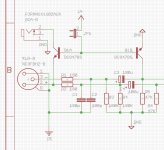
What about this? A simple dual NPN transistor in, say, SOT-363 package coupled with a two pin jumper (through-hole). When the jumper is fitted, both transistors conduct with one connecting SE hot to XLR pin 2 and the other grounding pin 3. Leave the jumper out for balanced operation. If someone wants to replace the jumper with a panel switch the pads are available for the wiring connection. It places a transistor in the SE signal path - does this dictate component choices?
What about this? A simple dual NPN transistor in, say, SOT-363 package coupled with a two pin jumper (through-hole). When the jumper is fitted, both transistors conduct with one connecting SE hot to XLR pin 2 and the other grounding pin 3. Leave the jumper out for balanced operation. If someone wants to replace the jumper with a panel switch the pads are available for the wiring connection. It places a transistor in the SE signal path - does this dictate component choices?
Attachments
Wouldn't it be great if Mr Self stepped in to share his view...?
I'll ask him ;-)
Actually, by reviewing SSAD 2nd ed., pg 508 fig 18.10 it is clear: if you leave the unused input open, the gain for the se signal is the same as for the bal signal, so no switching required.
That is with the se signal inserted directly at the +input through a small stopper resistor.
That though is a balanced circuit with a 5534 - yours is a instrumentation-type of circuit, I'm not sure I see through the differences in that circuit.
Jan.
That is with the se signal inserted directly at the +input through a small stopper resistor.
That though is a balanced circuit with a 5534 - yours is a instrumentation-type of circuit, I'm not sure I see through the differences in that circuit.
Jan.
Last edited:
Fig 18.10 is a circuit which deals with the volume imbalance between SE and bal by giving the bal connection a gain of 1/2 (by "increasing R1 and R3 to 20kR"). I'm prepared to ignore the volume imbalance. Both signals get buffered with unity gain in the above circuit. Yes, there will be a volume difference between the two connections but I don't expect me or anyone else to be bouncing back and forth between them and so the fact that the volume dial needs to normalise at a different setting for the same typical listening level is not something I am going to worry about.
An instrument amplifier typology is only useful is first stage gain can be set high so, following Self, that typology was rejected. Audio Power Amplifier Design Handbook puts the transition from discussing instrument amplifier typologies to unity-gain buffered differential amplifier typologies more clearly:
This then gets extended by doubling the amplifiers to get partial cancellation of their uncorrelated noise.
Obviously the exact scenario of combining unbalanced input with the ultra low noise balanced input (Fig 18.28) isn't presented in either text. The fact that many of the required components presented in Figs 18.1 (unbalanced) and 18.9 (balanced) are omitted from the later circuits "to improve the clarity" doesn't help either... For example, is R5 of Fig 18.10 needed here?
(Fig references are to the SSAD 2nd edition text.)
An instrument amplifier typology is only useful is first stage gain can be set high so, following Self, that typology was rejected. Audio Power Amplifier Design Handbook puts the transition from discussing instrument amplifier typologies to unity-gain buffered differential amplifier typologies more clearly:
We have seen that the instrument amplifier configuration is of limited use for audio work as it only gives an improvement in CMRR commensurate with the gain of its first stage. However, if we reduce it to a standard differential amplifier with a unity gain buffer on each input, we can reduce the value of the four resistors around the final differential amplifier, reducing their Johnson noise, and at the same time increase the input impedance presented to the outside world, and so possibly improve the CMRR.
This then gets extended by doubling the amplifiers to get partial cancellation of their uncorrelated noise.
Obviously the exact scenario of combining unbalanced input with the ultra low noise balanced input (Fig 18.28) isn't presented in either text. The fact that many of the required components presented in Figs 18.1 (unbalanced) and 18.9 (balanced) are omitted from the later circuits "to improve the clarity" doesn't help either... For example, is R5 of Fig 18.10 needed here?
(Fig references are to the SSAD 2nd edition text.)
Last edited:
PS: it's worth adding that I started this because I'd like to build Toni's 2 channel amp (SA2014). My DAC (Theta Digital Casablanca with Xtreme D-3 DACs) only has balanced outputs. So, for now at least, I care most about a balanced input stage. It made sense, however, to try to apply Fig 18.10 to the typology in Fig 18.28 and provide for both inputs. (My Fig references are to the SSAD 2nd edition text.)
Agree 100%.
I believe an R5-type stopper is good practise to avoid issues with input pin capacitance. I always use it, but of course YMMV.
I did build a fig 18.28 type circuit in SMD on a small PCB that also holds an XLR input connector but haven't tested it out yet. It looks complex but in reality the PCB is barely larger than the XLR, especially by placing parts on both sides. A bitch to solder though ;-)
Jan
Last edited:
It's interesting that elsewhere in the text there are no 'base stopper' resistors unless the 100R resistors shown in 18.1 and 18.9 also serve this purpose as well as the filtering of RF with their associated capacitors. Note, SE hot is injected ahead of all of these in the circuit above. (There are differences between the component values in 18.9 and those in 18.1, some of which are explained in the text. By injecting at pin 2 of the XLR we end up with a lower input impedance for the unbalanced than were it standalone with the components in 18.1 but it would seem liveable at 32kR.) Given in the unity-gain balanced input stage (with quad input buffers and four differential amplifiers) doesn't have the series resistors after the DC blocking caps like that of the basic balanced input stage, should stoppers be placed ahead of the unity gain buffers (i.e. another 8 resistors per channel)? ugh...
Last edited:
...
What about this? A simple dual NPN transistor in, say, SOT-363 package coupled with a two pin jumper (through-hole). When the jumper is fitted, both transistors conduct with one connecting SE hot to XLR pin 2 and the other grounding pin 3. Leave the jumper out for balanced operation. If someone wants to replace the jumper with a panel switch the pads are available for the wiring connection. It places a transistor in the SE signal path - does this dictate component choices?
Unfortunately it is not so easy to switch audio signals with such a simple transistor circuit (... and the left transistor would immediately die if the jumper is inserted...).
What I meant is: If SE RCA input is used, the neg. signal pin of XLR input should be shorted to signal ground by a relay. Of course in this case you should not connect any XLR source during SE RCA input mode and vice versa.
BR, Toni
I did build a fig 18.28 type circuit in SMD on a small PCB that also holds an XLR input connector but haven't tested it out yet. It looks complex but in reality the PCB is barely larger than the XLR, especially by placing parts on both sides. A bitch to solder though ;-)
Jan
Yeah I only placed the bypass caps on the bottom side of the board. As I started with the idea of two sets of connectors per board I didn't have to push for more optimisation of board space.
Even still, I'm thinking a stencil cut from Dura-Lar, solder paste and a hot plate may be easier than hand soldering everything. I've used it before and it works a treat. It's just a question of whether it takes more time to cut the stencil than hand solder.
Unfortunately it is not so easy to switch audio signals with such a simple transistor circuit (... and the left transistor would immediately die if the jumper is inserted...).
What I meant is: If SE RCA input is used, the neg. signal pin of XLR input should be shorted to signal ground by a relay. Of course in this case you should not connect any XLR source during SE RCA input mode and vice versa.
BR, Toni
If one only has to deal with shorting XLR pin 3 to ground when SE is used then the user can just use one of these
An externally hosted image should be here but it was not working when we last tested it.
An externally hosted image should be here but it was not working when we last tested it.
Saves a switch on the rear panel. Okay it grounds to chassis via pin 1 rather than signal ground...but it prevents a balanced connection being left in place. Of course, the user could forget but then they could forget to flick a switch as well.
Disconnecting the RCA connection to pin 2 for balanced use is a bit harder. If we don't care about this then we're done except for the question re base stoppers.
Last edited:
If one only has to deal with shorting XLR pin 3 to ground when SE is used then the user can just use one of these
Saves a switch on the rear panel. Okay it grounds to chassis via pin 1 rather than signal ground...but it prevents a balanced connection being left in place. Of course, the user could forget but then they could forget to flick a switch as well.
Disconnecting the RCA connection to pin 2 for balanced use is a bit harder. If we don't care about this then we're done except for the question re base stoppers.
IMHO not a good idea. Even if gain is only 1, you are going to insert noise from case to decoupled star ground into your audio signal. If you use RCA on pos. input you either leave neg. input open or must short it to signal ground to get lower noise.
BR, Toni
Ok.
I see my extremely basic error re passing the audio signal from RCA hot. Presumably the right side has the same issue. Before looking for miniature relays I'm hoping Jan gets a response from Mr Self re whether anything at all is required (and whether base stoppers should be added).
I see my extremely basic error re passing the audio signal from RCA hot. Presumably the right side has the same issue. Before looking for miniature relays I'm hoping Jan gets a response from Mr Self re whether anything at all is required (and whether base stoppers should be added).
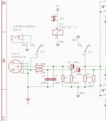
Perhaps this little DPDT relay is better suited to the task should switching be necessary
Omron G6K-2F-Y-TR DC12 at Mouser and its data sheet. 10mm x 7.8mm footprint in SMT. Could be mounted on the bottom side of the board.
Jumper in place or closed switch for SE use. Left open for Balanced use. Non latching. Draws about 100mW.
PS: I have seen base stopper resistors used with transistors but did not think them necessary at the input to op amps (occasionally at the output for stability control).
Attachments
Last edited:
Perhaps this little DPDT relay is better suited to the task should switching be necessary
Omron G6K-2F-Y-TR DC12 at Mouser and its data sheet. 10mm x 7.8mm footprint in SMT. Could be mounted on the bottom side of the board.
Jumper in place or closed switch for SE use. Left open for Balanced use. Non latching. Draws about 100mW.
PS: I have seen base stopper resistors used with transistors but did not think them necessary at the input to op amps (occasionally at the output for stability control).
This Variant with relay control looks good. Putting Pin 6 of the relay on the left/pos. side of C3 may be better to avoid any output DC offset caused by shorting R5 to signal ground.
BR, Toni
- Home
- Amplifiers
- Solid State
- Self's "5532 Low Noise Unity Gain Balanced Input Stage"