Can anyone let me know a sch for self biased Class A OPS without Vbe Multiplier just like pass F5 where without using Vbe multiplier the bias is set by a pot which is directly connected to rail and the Input of the OPS.
the actual problem is that when the room temperature shifts down the idle current fluctuates sometimes goes very low at times. Just need a solid standard fixed value based on the trim pot used. Since want to try various frontends would like to have a OPS with steady class A bias possibility.
Laterals are going to extinct as well.
Diamond buffer havent thought though
Laterals are going to extinct as well.
Diamond buffer havent thought though
If you take a look at the kx2-Amplifier (or the much older sx-Amplifier) on the hifisonix website, you can see a very simple single transistor + diode scheme that directly regulates a class A amplifier output stage standing current but will transition smoothly across to class AB at very low distortion when driving low impedance loads. A later amplifier, the ax-Amp, uses a Darlington transistor so avoids the diode for even better regulation over temperature.
Last time I checked Exicon laterals were still readily available. (I bought a bunch for a future class A power amp just a few months ago)Laterals are going to extinct as well.
Diamond buffer havent thought though
Diamond buffers are interesting, have used them in a variety of headphone amps and they can be scaled with some difficulty.
Thank you Andrew, couldnt find the sx amp schematic. Can you pls post it in here.If you take a look at the kx2-Amplifier (or the much older sx-Amplifier) on the hifisonix website, you can see a very simple single transistor + diode scheme that directly regulates a class A amplifier output stage standing current but will transition smoothly across to class AB at very low distortion when driving low impedance loads. A later amplifier, the ax-Amp, uses a Darlington transistor so avoids the diode for even better regulation over temperature.
With a class A emitter follower or source follower, the bias current can be stabilized by making the emitter or source resistors larger so that they drop more voltage. Unlike class AB, class A does not have an optimal voltage that minimizes distortion (with BJTs).
Ed
Ed
The kx2-Amp uses the same technique. See slides 17 to 20 in conjunction with the circuit diagram (also in the pdf).Thank you Andrew, couldnt find the sx amp schematic. Can you pls post it in here.
https://hifisonix.com/wp-content/uploads/2023/06/kx2-Amplifier-November-2022.pdf
A conventional Vbe multiplier is risky in a bipolar OPS class A amp because the feedback mechanism is primarily thermal and thus the output devices dVbe and sensor have to track accurately over a wide temperature range for tight standing current control. In a class A setup, direct regulation the OPS standing current is far more preferable.
See Nelson Pass also for direct regulation techniques for use with mosfets OPS.
Last edited:

Thank you andrew what I am looking at is the bias to be rock solid even for wide room temperature variation.
I guess pass uses more of resistor controlled fixed bias without tracking the output transistor/mosfet idle current through emitter resistor. But I also see him using NTCs in his design to stabilize when temperature is going up and in F5 he is also using Diodes from the rails to conduct when idle current goes beyond certain value.
only thing is that the transistor what you are using is BC550 package TO 92 which again needs clamps instead one can use ksc3503 as we can use a screw mount directly? anything to be varied in values?
If used with mosfet OPS do we require 220uF cap?
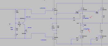
I have tried the above ckt that you have recommended but it seems oscillating even after the resistor values and capacitor values varied. Hence thought why not use a diode as is in the conventional vbe multiplier with the resistor from the output source resistor. It seems working but is there anything to be changed in the ckt attached?
Attachments
3281 power transistor?
It is mosfet output section
temperature coefficient is similar to BJT but not as drastic.
BJT will tend to over track or over compensate
thermally.
plenty of mosfet design with no thermal tracking
or just use simple diode.
Can also use to-92 because not mounted to heatsink
it wont over track like mounted BJT when tracking mosfet.
mounted bjt can use different circuit for less over tracking.
its overbiased push pull, just turn down the bias.
if under 60 watts then easy to set mosfet with set resistor.
Of course people will scream like crazy you cant do that.
least for normal A/b not overbiased
irf devives need little current to drive 610 drivers
not really needed. not sure if " speed up" capacitor is even useful
maybe use diamond boofer and over bias everything
irfp/9/240 dont need high 330 ohm gate resistor
that is for unstable lateral nonsense.
sorry MJ3281 was not used it was either BC550 or Ksc1381 used what is your proposed concept with just diode? especially with mosfets. The challenge here is the bias shouldnt change with ambient room temperature variation. Sometimes it can be 18 deg C and sometimes it can be 33deg C in hot conditions
Last edited:
For a mosfet output stage I’d use Nelson Pass’s opto-coupler method. If you search on that forum or ask the crew over there they can help you. The bias controller I showed is really for bipolar OPS and as you can see from the OPS standing current vs temperature and time, it’s very stable (low single digit % change over temp and time).Thank you andrew what I am looking at is the bias to be rock solid even for wide room temperature variation.
I guess pass uses more of resistor controlled fixed bias without tracking the output transistor/mosfet idle current through emitter resistor. But I also see him using NTCs in his design to stabilize when temperature is going up and in F5 he is also using Diodes from the rails to conduct when idle current goes beyond certain value.
only thing is that the transistor what you are using is BC550 package TO 92 which again needs clamps instead one can use ksc3503 as we can use a screw mount directly? anything to be varied in values?
If used with mosfet OPS do we require 220uF cap?
The 220uF 6.3 V cap is needed because at LF, when the output swings close to the V+ rail, the bias voltage collapses and distortion goes up. With the cap, you don’t get this.
I’m travelling now but when I get back I’ll see if I can find the NP bias circuit. Basically, you place the emitter diode of the opto across the source degeneration resistors (with appropriate current limiting resistor for the diode) and then use the coupler transistor to directly control the bias voltage to the mosfet gates. You will have to experiment a bit to get the right diode current limiting resistors and you can pre-bias the opto from the rails as well to alter the control slope.
Room temperature affects any device.
If higher ambient temperature is expected.
Then higher heatsink temperature is expected.
You increase the heatsink size.
Regardless thermal tracking is done at the heatsink.
As mentioned BJT temp coefficient is similar
but will over track or usually over compensate.
So there is numerous split bias topologies
which are used for mosfet.
Or you could use split bias with diode.
Or for additional accuracy.
Can use a BJT transistor as diode or use Mosfet
transistor as diode within split bias system.
Without extremely large post to explain
likely search for split bias VBE or split bias spreader
for non lateral mosfet
Otherwise as mentioned extremely simplified
way to not over compensate is use traditional spreader.
Use TO-92 placed close to heatsink. Not directly on heatsink.
The error caused from not directly mounting to heatsink
reduces over compensation.
so connecting the resistor from the OPS source resistor and connect via diode seems working why isnt it recommended for Mosfets?For a mosfet output stage I’d use Nelson Pass’s opto-coupler method. If you search on that forum or ask the crew over there they can help you. The bias controller I showed is really for bipolar OPS and as you can see from the OPS standing current vs temperature and time, it’s very stable (low single digit % change over temp and time).
The 220uF 6.3 V cap is needed because at LF, when the output swings close to the V+ rail, the bias voltage collapses and distortion goes up. With the cap, you don’t get this.
I’m travelling now but when I get back I’ll see if I can find the NP bias circuit. Basically, you place the emitter diode of the opto across the source degeneration resistors (with appropriate current limiting resistor for the diode) and then use the coupler transistor to directly control the bias voltage to the mosfet gates. You will have to experiment a bit to get the right diode current limiting resistors and you can pre-bias the opto from the rails as well to alter the control slope.
You could use it but I have not tried it with a mosfets OPS - only on bipolar OPS - whereas the Pass OPS bias arrangements are well tried and tested with mosfets.
https://hifisonix.com/wp-content/up...on-for-Audio-Amplifier-EF-Triples-V1.0231.pdf
I saw one of your links which speaks about the vbe multiplier
Now my question of taking the connection from the emitter resistor to the base of the vbe multiplier transistor seems quite interesting for me for the stability as it feels like a feedback..
Now how tight is the temp variation
consider if bias is set at room temp of 27degC then it reaches consider 42degC in one hour with idle current of about 0.5Amp per mosfet in consider 4 mosfets per rail.
Then, if the room temp drops to consider 16degC or reach to 40degC the idle current in the OPS shouldnt drop. Will the above sch of taking the connection from the OPS emitter / source resistor and then plugging back to the base of the Vbe multiplier would be very stable with consider even 0.05Amp of variation across 0.5ohm or 0.33ohm emitter resistor.
I see some amps loose the bias after temperature drops is that can be avoided by the above way of tieing the ops resistor to vbe multiplier?
- Home
- Amplifiers
- Solid State
- Self Biased steady Class A output stage without Vbe multiplier