Newer member here trying to learn about circuit building. I Just got my first blank pcb.
In the pic I provided there are some oval dots at the extreme end. Are those like power rails connecting the whole row of eyelets? If not what are they? Is the one row outside of the oval on both ends not linked to those ovals?
Does one work from a horizontal landscape or portrait?
I know these are basic questions. I have tried to find videos but none showing what I am asking for. Any help or references would be helpful and I am here to learn LOL
Thanks
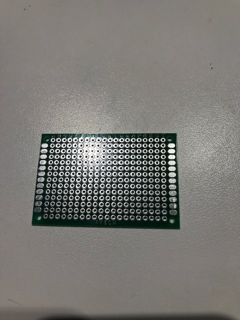
Last edited:
The dots are just tie points that are not connected to anything. You can use your meter to verify that.
That is a "pad per hole" board, with no interconnections between any of the pads.
Some boards do have some interconnections, which you can see.
That is a "pad per hole" board, with no interconnections between any of the pads.
Some boards do have some interconnections, which you can see.
Attachments

Last edited:
The oval pads are not usually connected to anything.
They are usually used for interconnecting boards, connecting wires for external circuits or sensors. They are also usually conveniently spaced to allow connection for headers such as screw terminals.
You can solder a line across them if you wanted to use them as a power bus for example.
Portrait or landscape depends on your layout - whatever fits best the application. Also a driver is often how the board fits best in the final enclosure.
And welcome!
AHH, so the connection is made by using solder or a wire? The orientation is subjective to the artist?
The ovals are used interconnect or add other things needing a bigger footprint?
oh and what do you mean by a "driver"?
The ovals are used interconnect or add other things needing a bigger footprint?
oh and what do you mean by a "driver"?
Last edited:
That's right.
There are some decent tutorials on soldering here if you need:
EEVblog #180 - Soldering Tutorial Part 1 - Tools - YouTube
There are some decent tutorials on soldering here if you need:
EEVblog #180 - Soldering Tutorial Part 1 - Tools - YouTube
AHH, so the connection is made by using solder or a wire?
Most of the time you can just use the component leads to make the connections.
Here's another video that might help explain the process:
How to solder grid style PCB / 555 PWM DC-motor driver (EEEL1-3) - YouTube
How to solder grid style PCB / 555 PWM DC-motor driver (EEEL1-3) - YouTube
Rayma and Avtech Thanks so much. I will post my finished board so you can tell me if it could be done better. I will test the circuits to see if it works!
Again Thanks
Again Thanks
I'd put some gas in the car before driving it.
It seems like the only way to get somewhere successfully.
But of course, it's an ignored point.
It seems like the only way to get somewhere successfully.
But of course, it's an ignored point.
The actual wire he uses in the video is what kind of wire? Is it called galvanized wire? It seems to be the same wire on the diodes I have. It is a bare wire. It bends. Where can I find that?
Last edited:
It's bare tinned copper wire like this:
Solid Soft Drawn 18AWG Bare Tinned Plated Copper Bus Wire 0.25lbs 59' Spool Roll 729440133184 | eBay
Or this:
https://www.newark.com/w/c/cable-wi...copper-wire/prl/results?st=tinned copper wire
Solid Soft Drawn 18AWG Bare Tinned Plated Copper Bus Wire 0.25lbs 59' Spool Roll 729440133184 | eBay
Or this:
https://www.newark.com/w/c/cable-wi...copper-wire/prl/results?st=tinned copper wire


- Home
- Design & Build
- Construction Tips
- Seeking Guidance Please