Andrew, yeah, but the higher Pdmax is usually assuming it's mounted on a fairly sizeable copper plane. I guess you could make a little PCB with copper on to act as a heatsink, and also as a carrier to take it up to TO-126/TO-220 pin spacing with some header pins
Yes, there's no denying that's been the case for some time here too but I was surprised to find these old parts in fair amounts throughout the middle east, for instance.Ian, problem is CRT's are obsolete so the parts are being discontinued. Im quite surprised its taken this long - most CRT driver boards use an IC such as LM2402.....
It would make sense to snap up any old TO126 or similar case BF4XX types which will be absolutely right for the job, at the right price, of course. This might help guys who otherwise can only buy garden variety components or fakes in their region. Buying on-line is not always a simple option in some countries either.
Sanyo (now Onsemi) 2SA1507/2SC3902 seem good.. Cob not as low as it could be but still pretty good. Maybe good drivers in a smaller amp too.
2SA1552/2SC4027 seems to be the same die, in a smaller package. The "TP" package is through hole, but could be a little too small for decent power dissipation.
2SA1418/2SC3648 also look good, lower Cob, but SOT89 - so clever heatsinking needed to get the 1.5W
2SA1552/2SC4027 seems to be the same die, in a smaller package. The "TP" package is through hole, but could be a little too small for decent power dissipation.
2SA1418/2SC3648 also look good, lower Cob, but SOT89 - so clever heatsinking needed to get the 1.5W
Ok so thinking about cascoding.
Firstly, if I cascode the Vas Transistor, I can use BC550 cascoded with MJE340.
But the "darlington" driver must still handle full voltage so 2n5551,
I'm not sure of what other transistor to use here.
Secondly, do I need to cascode the Vas CCS? or is it fine to use MJE350 on its own here?
If I cascode the Vas CCS, what impact does it have on the CCS, R4 need to change?
I've also increased the output to triple EF, since I'm cascoding Vas.
Regards
Attachments
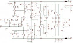

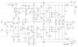
I'm struggling to stabilise the circuit in post 66.
It goes into low frequency oscillation.
Here is a revised circuit that has some changes, this one is fully working,
No ringing or funny visible oscillations from low input into heavy clipping.
Clipping on bottom half cycle sticks at 20khz driven into hard clipping.
But comes out of clipping perfectly, no unstability.
Output Power is 185W into 8R.
Sounds nice, highs come accross nice and clear, the way I like it.
Can someone please offer some suggestions on how to stabilise post66,
I want both VAS and VAS current source cascoded.
Thanks
Attachments
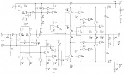
"what are the differences between sch 66 & 67? "
66 is the preferred connection for the cascode voltage reference to the emitter resistor rather than to the rail. 66 also has a cascode around the CCS for the Vas.
66 is the preferred connection for the cascode voltage reference to the emitter resistor rather than to the rail. 66 also has a cascode around the CCS for the Vas.
Do you think C4 and C9 (post69) will help, I've seen it on a NAD C372,
I'll make come changes next week,
Diode clamps look nice, another thing to try
thanks
I'll make come changes next week,
Diode clamps look nice, another thing to try
thanks
i.e. the cascodes exclude R4 & R20.................66 is the preferred connection for the cascode voltage reference to the emitter resistor rather than to the rail.................
What difference does this make?
IIRC it's similar in idea to the Lender circuit, a kind of local feedback if you will.
Its been a while since I read the Hawksford paper on this subject, my copy is at work (I think).
The APT is from about 1977, the Hawksford paper is from about 1988.
https://docs.google.com/viewer?a=v&...aNleyu&sig=AHIEtbTAbkaazXcW0c8yeuspUYKfxBvEuA
Read section 3.2 and see fig.6B
Its been a while since I read the Hawksford paper on this subject, my copy is at work (I think).
The APT is from about 1977, the Hawksford paper is from about 1988.
https://docs.google.com/viewer?a=v&...aNleyu&sig=AHIEtbTAbkaazXcW0c8yeuspUYKfxBvEuA
Read section 3.2 and see fig.6B
Last edited:
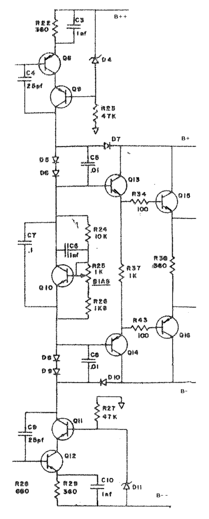
Finally.
Looks like my biggest problem, was initially being scared and running the amp from my bench 30V-0-30V supply, instead on 63V-0-63V it was designed for.
Most changes have been made, and I'm nearly ready to make the final boards.
This circuit posted is fully working,
Should I use a BC560 for Q20, instead of 2N5401.
I also think I might get rid of R28.
I've added D8 to help clipping behaviour.
With using matched pairs in ips and mirror, offset is very low.
But thinking of including a trim pot for offset.
Any comments would be appreciated on changes.
Regards
Attachments
Q19 & Q20 are current limiting devices. Neither should ever see high voltages. Low voltage devices are suitable.
How does D8 work?
Don't insert a trim pot in the emtter circuit of the LTP.
Better to look at VAS current trimming and/or adding a mirror trimming with a resistor from the bases to -ve rail.
Why are R41 & R42 different value?
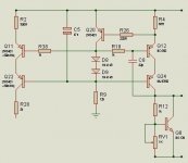
What compression did you set for your jpeg?
I find the values/details quite difficult to read.
How does D8 work?
Don't insert a trim pot in the emtter circuit of the LTP.
Better to look at VAS current trimming and/or adding a mirror trimming with a resistor from the bases to -ve rail.
Why are R41 & R42 different value?
What compression did you set for your jpeg?
I find the values/details quite difficult to read.
Last edited:
Without the diode the 'darlington VAS' struggles to come out of saturation.How does D8 work?
I have not seen this problem with a single transistor VAS, but when over driven really hard, I guess it could have a negative effect.
More experienced members would explain this better.
From my point of view, when the VAS transistors is driven with a large current from the IPS LTP then
the collector voltage of the vas transistor (Q3) drops quite low compared to its base voltage,
making the b/c junction forward bias, with diode added the current has a new path to flow, allowing Q3 to come out of saturation easier.
I'm not sure if I'm explaining well, I'm sure others will add to this.
Value of R41 needed to be low when cascode was for zener diode, the zener needed more current to pass zenerWhy are R41 & R42 different value?
knee. I increased R37 for about 2mA current, thinking id get get close to 0.7V per diode.
Value of R42 was originally the same as R41, But R4 feeds current to Q12 and Diodes D6/7,
that means that the value of R4 gets affected by the value of R42 (D6/7 current).
I decided to decrease current in D6/D7 to about 1mA which is still sufficient (greater than 20x Ib Q24)
As a side effect, max output before clipping was 185W with zener cascode, the circuit shown now has a
max output of 195W before clipping, but I still consider it 185W amplifier.
Circuit was exported as 1:1 screen res but at 1bit black/white bitmap.What compression did you set for your jpeg?
I find the values/details quite difficult to read.
Attached is a better resolution.
Regards.
Attachments

Same question
What is needed is more clarity, not more pixels.
Far too big.Why are R41 & R42 different value?
What is needed is more clarity, not more pixels.
Can't export as bitmap with low res and still be very visible.
On proteus default font is very 'thin' and small.
In other words, theres high jpg compression, saved as jpg from bitmap in photoshop at highest quality '12' jpg setting.
Even if I posted .bmp straight from proteus it would look the same.
Only other way is to export is pdf, I prefer jpg to export to web.
Regards
- Home
- Amplifiers
- Solid State
- Second attempt at Building my own amp from scratch