Final Steps - Projects!!
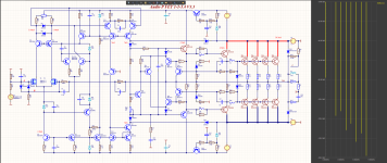
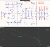
VFA P FET 1-1-3.4 V3.3
VFA P FET 1-1-3.4 V3.3
Attachments
-
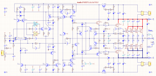 Audio P FET 1-1-3.4 V3.3 Sch.png154.9 KB · Views: 1,069
 -
Project Outputs for P FET 1-1-3.4 V3.3.zip899.6 KB · Views: 112
-
P FET 1-1-3.4 V3.3.zip6.7 MB · Views: 134
-
P FET 1-1-3.4 V3.3.PDF1.6 MB · Views: 141
-
P FET 1-1-3.4 V3.3 3D.pdf7.6 MB · Views: 170
-
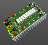 Audio P FET 1-1-3.4 V3.3 3D.png279.7 KB · Views: 477
 -
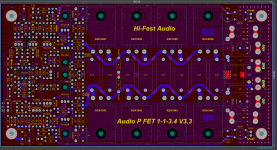 Audio P FET 1-1-3.4 V3.3 Pcb.png486 KB · Views: 485
Yes, everything has been tested live and many times.
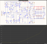
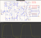
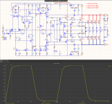
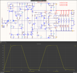
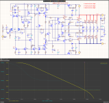
These are parameter simulations.
When measured, it showed distortions of the same order as in the simulations.
The simulation above is with an active load.
Down with speaker (speaker simulation model)
The PSRR in practice is significantly better than this simulation because of the additional active filter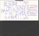
Attachments
Last edited:
Hi Sandy,
Thank you for sharing this design!
Could you please explain some details in your amplifier?
For example:
Thanks!
Thank you for sharing this design!
Could you please explain some details in your amplifier?
For example:
- purpose of D3/D4 diodes
- reasone for R11+R23 split
- working of U1/U2 + T5/T8 section
- purpose of D5/D6 + D11/D12
- working of the protection section
- anything else you would highlight maybe?
Thanks!
D3, D4 just don't allow T11, T18 to fully clog under restriction.
R11/R18 are 2 pieces because of the high voltage on them and to be low-voltage C11, C18 and with 2 times the large capacity.
Solder either U1 or U2 one is in a DIL8 housing the other in a SOT23-5 housing.
Depending on the preferred.
The op amp is a parallel DC channel to reduce the output DC offset of the amplifier.
The diodes D11/D12 do not allow T15, T16 to saturate under restriction (clip) And the diodes D5/D6 protect the base-collector transition of T29, T30 from unblocking under this restriction.
The protection is made in this way so as not to introduce distortion before it has really worked as it is with the standard ones that do not use D7, R31, D8, R32.
Dz8, Dz9 help to quickly close T31..., T32..., protecting them from burning during self-excitation at high frequency.
As well as reducing THD at high frequencies 100KHz.
All such things that ordinary Audio Designers have not reached yet.")
R11/R18 are 2 pieces because of the high voltage on them and to be low-voltage C11, C18 and with 2 times the large capacity.
Solder either U1 or U2 one is in a DIL8 housing the other in a SOT23-5 housing.
Depending on the preferred.
The op amp is a parallel DC channel to reduce the output DC offset of the amplifier.
The diodes D11/D12 do not allow T15, T16 to saturate under restriction (clip) And the diodes D5/D6 protect the base-collector transition of T29, T30 from unblocking under this restriction.
The protection is made in this way so as not to introduce distortion before it has really worked as it is with the standard ones that do not use D7, R31, D8, R32.
Dz8, Dz9 help to quickly close T31..., T32..., protecting them from burning during self-excitation at high frequency.
As well as reducing THD at high frequencies 100KHz.
All such things that ordinary Audio Designers have not reached yet.
I don't understand exactly which zeners you are writing about.
If we are talking about Dz8, Dz9 in the circuit are not used as zener diodes and their breakdown voltage is irrelevant.
They are used as ordinary diodes.
It's just that Zener diodes have a larger forward voltage and that's why they're used here.
In normal operation, there should not be a large current through them.
Their voltage in the forward direction should be slightly greater than that of the final transistors.
I have more than one way to connect two transistors.
Give a specific scheme for reworking all current generators so I can evaluate it.
And tell me in advance what the advantage of your proposed option is and how much it is an approximate improvement, (number)
How much higher output resistance would be obtained, and with what amount of elements, more or less like.
Yes, but in my case the reference voltage of DZ4 is used for 3 current generators. And its power comes from another power generator. T9/T7.
If I do as you suggest a T7 current generator, where will I get the reference voltage for the T12/T18 batteries?
Good in principle, but the question is what is the difference, in the specific case.
And this is understood only after calculations, and for which it cannot, at least with simulation.
But with a simulation not of the specific 2 transistors, but of the PSRR of the entire circuit.
Maybe the simulator in your hands is like a grenade in the hands of a monkey.
Simulations should only be done by people who can calculate a given scheme with a pencil and calculator.
U2 inputs don't you think affect the circuit even though the output is hanging in the air.
The circuit will never work with 2 op amps, 2 are put together just to have both SMD/DIL housings on the board.
R6 is always practically connected to ground simply with an external wire.
As you disconnected R13, the circuit will self-excite.
Simply, if you want to do electronics, first read more textbooks on the subject.
For the simulation, it is best to remove the op amp for the offset, it has no significant effect on the signal anyway.
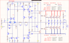
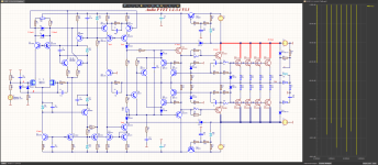
THD-500W THD-10W +PSRR -PSRR
THD-500W THD-10W +PSRR -PSRR
Attachments
Monkey business.
I made your model work. I replaced the zeners with voltage sources as no spice model. I had to rename bav21, you have the spice model bellow.
The THD with 25vp 8ohm is 0.01%.
Take off first all the extra outputs you added, start the simulation without steps, meas then make it sofisticated little by little.
What is square root transient analysis.
Attachments
The specific values of the frequency correction elements must be adjusted according to the specific transistors and even according to their specific models.
Allegedly identical transistors can be completely different models.
That's why I never use Cordel models. I use the latest models of the manufacturer and after checking.
Zener diode models should be explicitly checked very often are quite elementary with 0 dynamic resistance. It has little effect on THD but a lot of effect on PSRR.И
And live, the values are never the same as in the simulation!!!!!
There, everything is specified as it should be, but only by those who can count.
Attachments
- Home
- Amplifiers
- Solid State
- Sandy - Power VFA