Hello Everyone,
I've been trying to work on PCB trace routing, and have been cracking my head on the route of the feedback from output back to LTP.
The plan is to have 2 layer PCB, with top layer for signal and power and bottom layer for signal star-ground and local decoupling 0v.
I also intend to use SMD resistors as much as I can.
I used to run traces under THT resistors, and feedback usually trace back to LTP "jumping" across the VAS stage through the feedback resistor. But with SMDs the gap between the 2 pads are just too small to put through any trace................ I usually use 1mm trace for signal.
My questions are:
1. Is it wrong to run the feedback trace on the bottom layer, meaning the feedback resistor will be mounted underneath, and it will cross the VAS on the top layer with a gap of 1.6mm (thickness of PCB)?
2. If this is ok, should the feedback resistor 10kR be closer to the LTP (after crossing the VAS), or closer to the output (before crossing the VAS)?
Would appreciate your thoughts, many thanks.

Lowest impedance nodes (the output) have the longest leads.
Guards (guard tracks) only when more high output or high impedance nodes are close or involved.
Guards (guard tracks) only when more high output or high impedance nodes are close or involved.
I once routed an audio signal underneath a 7660 negative voltage inverter.
It put a 10KHz signal nicely on to my audio !
It put a 10KHz signal nicely on to my audio !
Thank you, I suppose you are also saying that the feedback resistor should be closer to the LTP.Lowest impedance nodes (the output) have the longest leads.
Guards (guard tracks) only when more high output or high impedance nodes are close or involved.
Hi Nigel, I'm not familiar with voltage inverter, but do you see my plan to be a problem? I can of course continue to use THT feedback resistor but I would really like to challenge myself with SMDs.
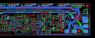
Run the FB trace on the edge of the board with a star ground compliment next to it. Current FB is on my new one , this will be refined.
Just look at a "wolverine" layout , (below) - part per billion THD.
The full swing output trace is "guarded " by the primary star ground along the bottom of the board. reducing the FB signal with a resistor and then
running it back to the LTP would make it far more influenced by any strong currents on the PCB.
I suppose if PPM/PPB performance is not a consideration , any scheme would work.
On the "slewmaster" , I ran a shielded (star grounded) coax from output to LTP (under the board -5ppm I got).
PS - "J3" is the FB point , runs under one of the star ground returns to the input board.
Attachments
Thank you for sharing. Not sure if I fully understand, Am I correct that R21 is the feedback resistor? My board has far less components. I had previously route the feedback trace on the same layer between THT components and did not have any issues. But the plan to use SMD parts has now limit my options to do that, unless I use the bottom layer as well.
Yes . R21 is main FB and R20 is TMC FB. Unless you are shooting for PPM , short of running your FB through the output coil or between
2 high current rail/returns , I won't add alot. Just keep high Z separate from low Z.
2 high current rail/returns , I won't add alot. Just keep high Z separate from low Z.
Thank you. Not sure if I totally understand as I have zero electronic education. But I read that output is usually low Z and the high Z is at the input stage. The feedback will cross one trace at VAS at 90 degrees, I hope this should be fine.
I'll give it a go anyways, probably worth investing some time and money for my learning.
I'll give it a go anyways, probably worth investing some time and money for my learning.
The more square the crossing, the less interlocking. Distance (with a jumper / wire) of the crossing will improve this even more, but then inductance is introduced too. An act of balancing!
Use 1206 size resistors and then there is plenty of space for a trace underneath. It may need to be narrow to pass underneath, but only for the short distance needed to get to the other side....with SMDs the gap between the 2 pads are just too small to put through any trace...
Douglas Self recommends avoiding SMD devices for the feedback path. His reference for this is a thread on this forum. However, if you dig in you can see that the issue was the voltage rating of SMD resistors. In general, the smaller the size, the lower to voltage rating.
I think the take away here is to check the voltage rating of these devices to ensure it works in your design. And in general, stick to 1206 or larger as these are usually safe. For example the the popular Susumu RG series 1206 package is rated at 200V but their smallest 0201 package is only rated for 30V.
I think the take away here is to check the voltage rating of these devices to ensure it works in your design. And in general, stick to 1206 or larger as these are usually safe. For example the the popular Susumu RG series 1206 package is rated at 200V but their smallest 0201 package is only rated for 30V.
One additional note, the Voltage Ratings for SMD devices can take a bit of detective work. With the Susumu RG devices I mentioned, the Max Voltage for the 1206 package is 200V. But you need to read the fine print. There's a note that states:
Assuming I'm reading this correctly, with a 1/4 watt 20K device, the actual rated voltage is 70.7V. For a 1/4 watt 1K this drops to 15.8V.
Not sure if this equation can be used with the actual power the device is passing, which would in theory raise the voltage rating.
Rated voltage is given by E= R x P E= rated voltage (V), R=nominal resistance value(Ω), P=rated power(W) If rated voltage exceeds maximum voltage /element, maximum voltage/element is the rated voltage.
Assuming I'm reading this correctly, with a 1/4 watt 20K device, the actual rated voltage is 70.7V. For a 1/4 watt 1K this drops to 15.8V.
Not sure if this equation can be used with the actual power the device is passing, which would in theory raise the voltage rating.
Try simulating the effect of adding a few picofarads between whatever parts you're crossing. In one design (simulation only), I had dual voltage + current feedback, where 1-5pF across the voltage feedback resistor made big changes in the stability at 30kHz+. So it may have also been sensitive to picking up noise from nearby components.
1 or 2 through-hole parts in a mostly SMD design is no big deal though. "Form follows function". Very respectable to take care of those details, IMO.
1 or 2 through-hole parts in a mostly SMD design is no big deal though. "Form follows function". Very respectable to take care of those details, IMO.
One additional note, the Voltage Ratings for SMD devices can take a bit of detective work. With the Susumu RG devices I mentioned, the Max Voltage for the 1206 package is 200V. But you need to read the fine print. There's a note that states:
Assuming I'm reading this correctly, with a 1/4 watt 20K device, the actual rated voltage is 70.7V. For a 1/4 watt 1K this drops to 15.8V.
Not sure if this equation can be used with the actual power the device is passing, which would in theory raise the voltage rating.
Hello Brian,
I had a closer look at the datasheet, and my impression (I could be wrong) that the formula E= √R x P was stated in the context of the testing condition.
I'm not 100% sure what I'm talking about, but if I apply that formula to what my condition (1W 47R), it would give only 6.7V which is incredibly low.......... I'm actually looking at the HRG 1W with max voltage of 200V.
It depends how much feedback your circuit uses. The higher, the more sensitive the LTP node is to noise, so you want short traces (traces are aerials). IOW place the fb resistors close to the LTP base.
Nelson's circuits are probably low feedback.
Nelson's circuits are probably low feedback.
My understanding is, resistors working under lean duty cycle conditions can be subject to very high voltages and still safely stay well within the rated power. This is because the rated power in the datasheet means to be of RMS value, not of instantaneous. However, despite the lean duty cycle and safe rms power dissipation, that "very high" voltage shouldn't be allowed to go so high that it may cause the voltage differential in the winding patterns of the element to jump gap, or material to deteriorate, or other failure mechanisms to kick in. A maximum voltage rating is then needed, and this maximum voltage rating can have little to do with the resistors resistance value or its power rating.I'm actually looking at the HRG 1W with max voltage of 200V
Thanks for the note, will put the FB resistor as close to the LTP as practical.It depends how much feedback your circuit uses. The higher, the more sensitive the LTP node is to noise, so you want short traces (traces are aerials). IOW place the fb resistors close to the LTP base.
Nelson's circuits are probably low feedback.
Not sure if this is a high or low feedback, from the output is a 12kR back to the LTP and a 470R + 100uF to the ground.
- Home
- Amplifiers
- Solid State
- Routing of Feedback from Output to LTP