
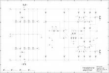
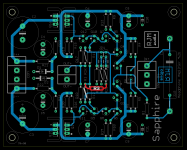
Sorry, that schematic is out of date. At some point an updated version I made got discarded and I use an older version in the documents by mistake. Always use the excel BOM "design manual" for the up-to-date (and vetted) parts lists.
Sapphire web page
I have made the needed edits and the schematic should now match the BOM.
With 1 ohm and 100 ohm your bias current will run a little high I think.
Sapphire web page
I have made the needed edits and the schematic should now match the BOM.
With 1 ohm and 100 ohm your bias current will run a little high I think.
Attachments
Last edited:
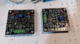
Thanks for the info. I made the boards last week, at the same time I downloaded the files from the site.
I will make the measurements in the afternoon and come back with the results.
I will make the measurements in the afternoon and come back with the results.
Hello,
The problem is on the pcba which heats up less. On R19 I have a voltage of 70mV.
I changed the 1 Ohm resistors with 4.7 Ohm and 100 Ohm with 220 Ohm on the board that was heating up harder and it turned out that this board is OK.
On R19 I have a voltage of 170mV.
Now that I have fixed the fail card, where do this problem come from?
The measurement is:
R19, R20 - 68 mV
R19 - 720 mV
R20 - 730 mV
R17, R18 - 83mV
R11 - 102mV
R12 - 100mV
R2A - 29mV
Thanks.
R19, R20 - 68 mV [4.7 ohm, 14.5 mA]
R17, R18 - 83mV [4.7 ohm, 17.7 mA]
R11 - 102mV [221 ohm, 0.46 mA]
R12 - 100mV [221 ohm, 0.46 mA]
(I assume R19 - 720 mV [4.7 ohm, 153 mA], R20 - 730 mV [4.7 ohm, 155 mA] is incorrect since R19 20 can't run 150 mA unless R18 R19 are passing 150 mA too)
The above results are about half of what is expected, which should be 35mA,38 mA, 1mA and 1 mA respectively.
Generally if a transistor in this circuit blows or is connected incorrectly, the whole amp stops working. I was playing in LTspice to see if I could reproduce the bias current you measured, the only way I could was to change R11 and R12 to 100 ohms instead of 221 ohms. So I would check those resistors to see if they are the correct value.
Actually, the bias current calculation is pretty simple.
The voltage rails are 11.5 V, so, ignoring Vbe drops, you have 1k+221 ohms (R11 amd R13) connected over 11.5 V, which draws about 0.8 mA of current.
Since the bases of Q10 and Q12 are tied together, the voltage across R11 and R17 must be the same. The current ratio is therefore just the ratio of the resistances, 221/4.7 = 47x , so if 0.8 mA flows through R11 you can expect 0.8 x 47 = 40 mA through R17. R15 and R19 control how much of that current flows through Q13 and how much flows through Q12.
Hello,
I found the cause of the problem.
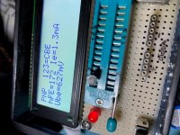
Q3 and Q9 had much lower Hfe than the other transistors.
I noticed that an ok transistor has Hfe somewhere at 500 and these two Q3 and Q9 had Hfe somewhere at 170-180.
After changing those transistors the problem disappeared, the voltage drop on R19 and R20 is 0.175 mV (37 mA).
Thanks for the help RJM.
This amplifier sounds great. I will use the Audio-Technica ATH-AVC500 headphones.
I found the cause of the problem.
Q3 and Q9 had much lower Hfe than the other transistors.
I noticed that an ok transistor has Hfe somewhere at 500 and these two Q3 and Q9 had Hfe somewhere at 170-180.
After changing those transistors the problem disappeared, the voltage drop on R19 and R20 is 0.175 mV (37 mA).
Thanks for the help RJM.
This amplifier sounds great. I will use the Audio-Technica ATH-AVC500 headphones.
Attachments
Hello,
The problem is on the pcba which heats up less. On R19 I have a voltage of 70mV.
I changed the 1 Ohm resistors with 4.7 Ohm and 100 Ohm with 220 Ohm on the board that was heating up harder and it turned out that this board is OK.
On R19 I have a voltage of 170mV.
Now that I have fixed the fail card, where do this problem come from?
The measurement is:
R19, R20 - 68 mV
R19 - 720 mV
R20 - 730 mV
R17, R18 - 83mV
R11 - 102mV
R12 - 100mV
R2A - 29mV
Thanks.
A mistake has crept in here
R19, R20 - 68 mV
R19 - 720 mV
R20 - 730 mV
R17, R18 - 83mV
R11 - 102mV
R12 - 100mV
R2A - 29mV
That's right:
R19, R20 - 68 mV
R15 - 720 mV
R16 - 730 mV
R17, R18 - 83mV
R11 - 102mV
R12 - 100mV
R2A - 29mV
The correct values are approximately,
R19, 20 - 35 mA / 165 mV
R15, 16 - 4 mA / 0.9 V
R17, 18 - 39 mA / 183 mV
R11, 12 - 1 mA / 221 mV
R19, 20 - 35 mA / 165 mV
R15, 16 - 4 mA / 0.9 V
R17, 18 - 39 mA / 183 mV
R11, 12 - 1 mA / 221 mV
High tolerance of the components used.
@rjm
Can you post the diagram from the simulator? I hope it will help those who want to build this amplifier.
@rjm
Can you post the diagram from the simulator? I hope it will help those who want to build this amplifier.
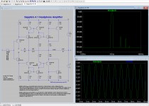
Please go ahead. It's been a few years since I've last fiddled with it and I'm always open to suggestions.
1. Bias current through Q1,2 tripled.
2. Switch to open loop output stage (this was always an option on the sapphire boards btw)
3. Slight reconfiguration of the feedback loop to ... what can we call this? A current mirror?
The latter change (3) interests me. Can you explain the functional differences between this and a conventional voltage divider?
Not so much a suggestion. More a hint.
I have been using this for many years, in a few different favours.
This converts the circuit from one with quite a bit of NFB, to one that is open loop.
Or what we call Zero Global Feedback. i.e. completely open loop, not just output stage.
Like in all Ayre designs.
XEN ZGF Portable Headphone Amplifier
Easy to try. Different sound.
UTHAiM -- Just for Fun
Cheers,
Patrick
Thanks.
It would seem that once the output stage is taken out of the feedback loop, there's no measurable benefit to adding feedback from the I-V converter to the input stage vs. local degenerative feedback applied to arrive at the same voltage gain.
Which probably shouldn't be a surprise since distortion is dominated by the output stage, but it hadn't occurred to me.
If anyone want to try, R3 would be connected as a flying bridge, as shown in the attached image.
Attachments
> distortion is dominated by the output stage
If your spice models are accurate then this is not quite true :
Fourier components of V(output)
DC component:0.000942295
Harmonic Frequency Fourier Normalized Phase Normalized
Number [Hz] Component Component [degree] Phase [deg]
1 1.000e+03 1.200e+00 1.000e+00 -0.17° 0.00°
2 2.000e+03 4.022e-05 3.352e-05 -121.17° -121.00°
3 3.000e+03 2.063e-05 1.720e-05 20.80° 20.96°
4 4.000e+03 2.077e-07 1.731e-07 -34.21° -34.05°
5 5.000e+03 2.629e-07 2.191e-07 -86.98° -86.81°
6 6.000e+03 2.229e-07 1.858e-07 -77.34° -77.18°
7 7.000e+03 2.209e-07 1.841e-07 -74.81° -74.64°
8 8.000e+03 2.189e-07 1.824e-07 -72.61° -72.44°
9 9.000e+03 2.164e-07 1.803e-07 -70.30° -70.13°
Total Harmonic Distortion: 0.003768%(0.014736%)
At the output of the VAS before the output stage (out2)
Fourier components of V(out2)
DC component:0.00392778
Harmonic Frequency Fourier Normalized Phase Normalized
Number [Hz] Component Component [degree] Phase [deg]
1 1.000e+03 1.279e+00 1.000e+00 -0.17° 0.00°
2 2.000e+03 3.832e-05 2.997e-05 -125.32° -125.16°
3 3.000e+03 2.017e-05 1.577e-05 22.81° 22.98°
4 4.000e+03 2.223e-07 1.739e-07 -34.60° -34.44°
5 5.000e+03 2.801e-07 2.191e-07 -86.11° -85.95°
6 6.000e+03 2.372e-07 1.855e-07 -77.34° -77.17°
7 7.000e+03 2.351e-07 1.838e-07 -74.81° -74.64°
8 8.000e+03 2.330e-07 1.822e-07 -72.60° -72.43°
9 9.000e+03 2.302e-07 1.801e-07 -70.29° -70.13°
Total Harmonic Distortion: 0.003387%(0.014643%)
IMHO the VAS dominates the distortion spectrum.
Cheers,
Patrick
Right, voltage amplification is the limiting factor as long as the load remains benign.
Funnily enough, I think I knew this back in the day, but I noticed that your circuit doesn't show any increase in harmonic distortion even dropping the feedback loop around the IV stage so ... why is that?
Funnily enough, I think I knew this back in the day, but I noticed that your circuit doesn't show any increase in harmonic distortion even dropping the feedback loop around the IV stage so ... why is that?
Many parameters you can choose to change the distortion spectrum in the VAS.
I'll let you have fun playing with it yourself first.
Costs nothing in Spice.
And you already have one example.
😉
Note that I am using 1Vrms into 32 ohm as standard benchmark.
See also :
Pass Labs HPA-1 headphone amplifier Measurements | Stereophile.com
Patrick
I'll let you have fun playing with it yourself first.
Costs nothing in Spice.
And you already have one example.
😉
Note that I am using 1Vrms into 32 ohm as standard benchmark.
See also :
Pass Labs HPA-1 headphone amplifier Measurements | Stereophile.com
Patrick
- Home
- Amplifiers
- Headphone Systems
- RJM Audio Sapphire Desktop Headphone Amplifier