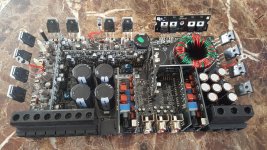
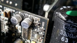
Hey guys, first time poster, I bought my first RF in 2014 and fell in love. Best amp I've ever owned. However, over the last snow storm, I had to disconnect my sub in a hurry and the wire that was bridged on channels 3 and 4 ended up in a puddle. Dead short. I didn't realize until I smelled the magic smoke. I quickly turned it off, but not quick enough. Now on this amp, looking at the PCB with the terminal ends towards me, the toroidial transformer is on the right, speaker outputs on the left and power/ground on the right. There are 4 transistors on the right that were so fried that the gate pin on each one was burned off. Actually, one survived, second in from afar. Then we have the rectifiers and 317/337 regulators going around counter clockwise. Next we have 36p15 and 46n15 respectively 3 more times, total of 4 of each. So 12 mosfets in all. I am wondering what the 4 mosfets on the right are for, the ones that burned out, as they are all the same n channel. I would think that you would need pos and neg equally, but I don't know much about amps, I'm learning. Anyway, my main goal is to fix it, I replaced the 4 bad transistors on the right. But when I plugged it in to test, the one farthest got very hot to the touch. Also, on the AB Power Supply daughter board, (third vertical board in from the right), 2 transistors on it are fried. I ordered them also and I'm waiting for them to arrive. They were hard to find. Do you think this amp is fixable? I love it so much and I purchased another, but it's a downgrade punch, so I am devastated. Something so simple and so stupid really tore this amp up! Any info you need or pics, please just ask, I am more than happy to provide them. Thanks to all in advance who provide anything at all for me.
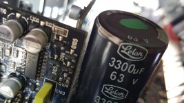
Oh, I forgot to tell you's, I believe all of the mosfets along the top are bad also. I did the meter test and they are all shorted. So I ordered them also. So at this point, my plan is to replace all of them on the top and replace the 2 transistors on the daughter board I mentioned and then replace the cap I took out to gain access. Now could all of these items cause that far mosfet on the right to overheat like that? That is my main worry b/c I cannot find anything else wrong at least visually. I did test all of the large caps and they all show their rated uF. And I tested some other random things, such as the bias resistors.
Oh, I forgot to tell you's, I believe all of the mosfets along the top are bad also. I did the meter test and they are all shorted. So I ordered them also. So at this point, my plan is to replace all of them on the top and replace the 2 transistors on the daughter board I mentioned and then replace the cap I took out to gain access. Now could all of these items cause that far mosfet on the right to overheat like that? That is my main worry b/c I cannot find anything else wrong at least visually. I did test all of the large caps and they all show their rated uF. And I tested some other random things, such as the bias resistors.
Attachments
Last edited:
Read the basic repair guide in its entirety. Link in sig line below.
If the power supply FETs (4 on right) failed, their gate resistors may have failed as well.
The failed driver transistors (on 3rd board) are likely the PNP transistors. The NPN transistors that work with them sometimes fail.
When you get the drivers replaced, connect only remote and ground and measure the DC voltage on the power supply FETs. Black probe on leg 3, red on 1. Post the voltage on all 4.
The driver transistors are very common. Why were they hard to find and where did you buy them from?
Thank you Perry, I appreciate it, I am doing it right now! You seem to be the go-to person on this forum, I appreciate any advise. <reading. . . . . >
Damn, I guess I didn't read the rest of your post, I jumped right into the reading, which, by the way is totally awesome. I am really enjoying the read. Very interesting stuff, but I notice there's not much about Mosfets. . . Only FET's. As for the driver transistors, I looked them up, they have W2A printed on them and two different sites said two different things. One had a part # that was obsolete in mouser/digi-key. Then I had to trust that the other one was right. So I went with that.568-6539-1-ND is the part number in digi-key. I will do exactly as you say and post it. People have a way of testing transistors where you take the MM and put neg to source and pos to gate quickly then to drain and you should hear it short then if you drain the V with your finger or resistor, it will stop. Is this accurate? I have tried it on known good mosfets and it does not work that way. Thanks for your help btw. Back to reading!
Damn, I guess I didn't read the rest of your post, I jumped right into the reading, which, by the way is totally awesome. I am really enjoying the read. Very interesting stuff, but I notice there's not much about Mosfets. . . Only FET's. As for the driver transistors, I looked them up, they have W2A printed on them and two different sites said two different things. One had a part # that was obsolete in mouser/digi-key. Then I had to trust that the other one was right. So I went with that.568-6539-1-ND is the part number in digi-key. I will do exactly as you say and post it. People have a way of testing transistors where you take the MM and put neg to source and pos to gate quickly then to drain and you should hear it short then if you drain the V with your finger or resistor, it will stop. Is this accurate? I have tried it on known good mosfets and it does not work that way. Thanks for your help btw.
Wow, you really know your stuff, this is a fantastic read, I am learning a hell of a lot so far! Anyway, I wanted to tell you that I also have a scope and a power supply. And yes, I am one of those ppl who have been using it for years and have no idea what the hell I'm doing. I've been into electronics for about 5 years now and know my way around a PCB, etched a few of my own designs, but you are an expert, I stepped into a huge pile of s**t meeting you on here. I actually feel like I'm going to fix this thing. I'll get back when I'm done reading. I've been across this page before during research, but when I saw the advertisement, I assumed it was just to try and sell something. But now, I actually want to buy the tutorial!
Man, this stuff is GOLD. Amazing, I cannot believe how much I'm learning! I'm taking notes and everything!
MOSFET = FET for the large transistors. There are other FETs like JFETs but you don't deal them much in amp repair (not compared to large FETs). Look up the datasheets for more information on various components.
2A is the relevant part of the mark. The one you ordered is OK. MMBT3906 is what's on most of the Rockford diagrams for drivers. I generally use the MMBTA06 and MMBTA56 for replacement drivers but the originals work perfectly fine
I doubt that Rockford has released the diagram for you amp. The following diagram is somewhat similar, especially in the power supply drive circuit.
http://www.bcae1.com/temp/rockford - punchP8004SCH-4707-D.pdf
You can test the FETs that way but for the FETs used in the power supply and output stage, you generally get leakage from the gate to the other legs when the FETs fail. IF you ever read anything other than infinite resistance from the gate to either outer leg, the FET is defective. Not all meters drive the same voltage to the probes so what works for one meter doesn't work for other meters.
For definitive testing, the FETs have to be out of the circuit.
Follow all links from the basic repair page.
If you don't know what you're doing with your scope, read page 73 of the site. Read and re-read the 'best initial settings' section.
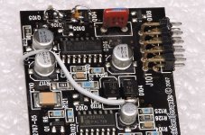
Just a quick question, why are your example amp driver transistors so big and mine are tiny smt transistors? I feel that there has been a miscommunication or something. . .
Wow, you are a HUGE help! Thanks man, I feel like I should be paying you! Not only are you a huge help, but you respond quickly also. I am definitely buying your tutorial if only out of reciprocation. That punch schematic looks like a huge amp! That's awesome that you got your hands on that. You'd think RF would guard them like gold.
Sorry for posting so much, but I just cannot believe how everything in this read is corresponding to me and my amplifier! It's like you're reading my mind and looking at my amp at the same time!
The size of a transistor is often determined by the amount of heat that it has to dissipate. The drivers in this amp have to dissipate very little heat so they don't need to be large. If you look at the datasheet below, you can see that the MPSA06 transistor has 2 other versions that are different sizes. The piece of silicon is the same for all 3 but the case determines the amount of power (in the form of heat) that they can handle.
Attachments
Thank you for the clarification Perry. I knew about heat dissipation, but I thought the difference there was way too big, very big difference in size! I'm actually shocked that those little buggers are drivers! But like you said, not much heat to sync. Anyway, I have pretty much completed the read. It's just a matter of waiting for the parts now. They will all be here by Tuesday. The W2's are coming tomorrow and I just ordered the top row of output transistors yesterday as I only realized yesterday they were blown. I'm not sure, but I think I may have messed up a trace or 2 on the power supply board. I need to clean it better to see. I tried alcohol, but to no avail, can I use acetone on a pcb? If I did mess up a trace, the only other thing I can think of is using a trace pen I have or soldering a small wire to the end of the trace to the transistor. Do you have any tricks for that? It was tough to get to as it is. And getting the daughter board out would be impossible without a hot air rework station. Something I've been meaning to get. Only thing I do have is a hot air gun, (paint stripper), which I use when salvaging old pcb surface mount components.
To remove the boards... ChipQuik. Nothing works better.
Acetone and either cotton swabs or a toothbrush are good for cleaning the board.
Stand the amp on edge to work on the driver board.
For examining the board, the Dr. Mom otoscope (walmart) is great. Don't let any solvent get on the lens. It's VERY easily damaged.
https://www.walmart.com/ip/Doctor-Mom-Otoscope-1ct/17324995
Never use a pen to repair traces. Use wire and fix them to the board with something like GOOP to prevent vibration from breaking the wire at the solder connection.
It's common on some driver boards for the board to be damaged. The attached images show part of the repair for a board with burned trace. The wire is a strand of computer ribbon cable.
Attachments
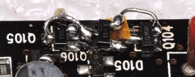
The base and emitter legs connect to the base and emitter of the transistor above Q104. The collector of Q104 goes to ground.
I just tested it with my meter Perry, I put a probe onto the copper colored lines and to the pads themselves and they are indeed connected, I guess the solder mask just came off, that's all. So I'm all good, all I need to do is install the transistor. I am wondering if this one is bad though, it's just got like a cavity in it. . . Q103 I believe it is. . .
Attachments
- Status
- Not open for further replies.
- Home
- General Interest
- Car Audio
- RF Power T600 Short Plz HELP!!!