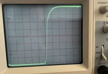
Here is a test waveform with an Exicon lateral MOSFET. The rise time test is an ECX10N20 driven by 0 to 2 volt (no negative zero crossing) square wave at 100khz , with a 470 ohm drain load from a 42 v power source. Scope is at 5v / div for detail. The tiny step at the start of rise is because there is no bias when signal source is at 0. I wanted to see the characteristics from a zero start. It is one fast device.
Attachments
Those were good parts. Unfortunately they fell a little short on current. The half amp rating was ok for hifi receivers and integrated amps, and of course hobby builds, but at least 1.5 amp rating would have been needed for professional amplifiers. They had the 8 amp devices, I never understood why they didn't make a driver with an amp or two rating.In the old days I did similar driver tests and found the hitachi LatFETs 2SK213/2SJ79 being superior to bjt drivers. I used one pair of these to drive 36 pairs of Hitache TO-3 laterals in a 5kW Monoblock. Sadly these latFETs disappeared from the market for a long time.
Transistorlegacy, thanks for the good info!
For a moment I was scratching my head thinking how can they omit the isolators between mosfets and heatsink in the soundcraftsmen amp. Then I remembered that some amps with the lateral mosfets have no degeneration on the outputs.
For my build I am thinking of finding some surplus PC processor heatsink/fans and use one per mosfet, no electrical connection from the aluminum to anywhere so no parasitic capacitor. I will not need any isolation, I will build on a plank of wood.
Thanks,
Alex
In common source circuits using a live heatsink design, no isolation is need if there is a real case to heatsink connection, as with a TO-3.Transistorlegacy, thanks for the good info!
For a moment I was scratching my head thinking how can they omit the isolators between mosfets and heatsink in the soundcraftsmen amp. Then I remembered that some amps with the lateral mosfets have no degeneration on the outputs.
For my build I am thinking of finding some surplus PC processor heatsink/fans and use one per mosfet, no electrical connection from the aluminum to anywhere so no parasitic capacitor. I will not need any isolation, I will build on a plank of wood.
Thanks,
Alex
The plastic case MOSFETs don't connect well enough to prevent oscillation, and ceramic isolators must be used, or undesirably high value gate resistors. The Exicon MOSFETs are faster and lower source resistance than originals. If you have any capacitor effect between case and heatsink with multiple devices, it will reliably oscillate. Even old MOSFET amplifier designs were marginally stable, hence how many need repair. I always add ceramic insulators on such repair job, unless it has good live heatsink connection like a Soundcraftsmen , the result is stable even with no zobel network.

I scored some of those in an auction! 😎TO-3
This was here in brazil of all places! They are almost impossible to find.
https://ibb.co/nbPL5CN
In common source circuits using a live heatsink design, no isolation is need if there is a real case to heatsink connection, as with a TO-3.
I think you mean source follower, aka common drain.
(Obviously the heatsink must be isolated from ground / chassis.)
I think everybody that read this got it already, but just to be clear, the case of the mosfets is the source terminal AND there's no source resistors in the design.
Last edited:
In reference to the ESP P101 amp build. Output osc. discussed by Rod E.
"Finally, the output section uses a conventional Zobel network. If desired, this can be followed (right at the speaker terminals) by a small inductor with a paralleled resistor, and finally a second Zobel network at the output. This is intended to decouple the amplifier from highly capacitive loads and ensure stability under all normal operational conditions. The use of ultra-low inductance (very high capacitance) speaker leads is not recommended, although the additional output network described will prevent oscillation in most cases. The inductor can be quite small (around 5-10µH is about right), and must be shunted by a parallel resistance of between 2.2 and 10 ohms (10µH gives a -3dB frequency of 71kHz with an 8 ohm load)."
Since I'm using double dye T03 Exicon outputs mounted on the heatsinks and hardwired (about 5 inches) to the boards, I thought I would use his suggestion and wire the parallel inductor and resistor (5uH / 5 Ohm) at the speaker terminal. What would be any downside to NOT using the second
Zobel. Duplicating R18, C8, and C10. I'm assuming that is what he meant by a second Zobel at the output.
Is there an online calculator for determining the -3dB cutoff freq. as Rod did?
Hello sirI found a few older threads here mostly regarding older parts, and some stability solutions which do not yield good results with parts now available. So I figured we could have a thread dedicated to using the Exicon mosfets in novel ways I have not seen mentioned here.
Like most people, I encountered oscillation when using multiple devices, and tried the usual higher gate resistor values, and capacitors. By the time these measures could help, the amp was too slow, which in turn caused feedback loop stability issues. So, I did some research and found that that the culprit is loop currents between case and source leads with multiple devices. When TO-3 devices are mounted to a live heat sink, and source lead trace goes right to one of the case screws like the Soundcraftsmen PCR800, it's all good.
But that doesn't happen with the plastic case devices. They usually don't make a good connection with the heat sink at all, but instead form a good capacitor - perfect Colpitts oscillator ! And if you used mica insulators, it's real bad. Here is the solution : isolate the devices from heat sink with aluminum oxide pads such as ones from Aavid, found at most major parts vendors. I then used 330R gate resistor and 47pf right from gate to drain on N channel device, and 220R gate resistor, and 100 pf cap for P channel device. Easily obtained 80 v/us speed with stability. Even works well dual differential front ends. For the double die devices , I found that 220R gate resistor and 68 pf across gate and drain for N channel, and 150R , 150 pf for P channel worked well. These parts must be on each device, with capacitors right at gate / drain leads.
Now here is the good part, it turns out that lateral MOSFETs make great driver stages. Way faster than using large power transistors, and far better than building up triple Darlingtons.
Any good VAS stage will drive one pair of the single die Exicons very well. The sound is fantastic. MOSFETs break the path of current draw being passed all the way back to input stage as happens with pure bipolar design. If anyone is interested in this subject, I would be happy to share more info, and schematics as well.
I'm looking for a way to get 3-4 pairs of 20N20/20P20 to work stably in parallel, and I want to keep the high-speed characteristics of the MOSFETs as much as possible, lose as little effective bandwidth as possible, and maximize the amount of negative feedback available.
They oscillate easily, as many have encountered. I've tried increasing the gate resistance, and while this solves the local oscillation problem, it also makes the MOSFET output stage too slow with a huge loss in distortion performance.
Until one day, I found this post😛
I was wondering, when you try to connect more 20N20/20P20 in parallel, do you also use the compensation values you shared?
If I want to not slow down the MOSFET as much as possible, is there a more optimal way of compensation and compensation values?
thank you very much
I didn't see this post until now... Yes the compensation values listed right in the start of this thread are for each device. I listed the values for single and double die devices. The recommended ceramic insulator is important. This solution has attained 100 v/us slew rate for me. I found this solution to be better than the alternatives, such as using a live heat sink and and bonding the source lead right to the heat sink (emulating the TO-3 mounting), or using large bypass capacitors from drain to ground plane at every device, or the dreaded heavy compensation where the reduced slew leads to phase lag problems, leading to needed more compensation in more stages.Hello sir
I'm looking for a way to get 3-4 pairs of 20N20/20P20 to work stably in parallel, and I want to keep the high-speed characteristics of the MOSFETs as much as possible, lose as little effective bandwidth as possible, and maximize the amount of negative feedback available.
They oscillate easily, as many have encountered. I've tried increasing the gate resistance, and while this solves the local oscillation problem, it also makes the MOSFET output stage too slow with a huge loss in distortion performance.
Until one day, I found this post😛
I was wondering, when you try to connect more 20N20/20P20 in parallel, do you also use the compensation values you shared?
If I want to not slow down the MOSFET as much as possible, is there a more optimal way of compensation and compensation values?
thank you very much
After 3 decades I realized a certainty : once you slow down an amp, you have to slow it down a lot to keep it stable. That's why so many amps are under 20 v/us.
- Home
- Design & Build
- Parts
- Revisiting lateral MOSFET stability