The first amplifier I ever built as a youngster was from a kit, and was around 10 watts/channel from a pair of AD149 germaniums. I was hooked though 
I began taking magazines such as Practical Wireless, and it was here some 40 years ago that a diy project captured my imagination and so I had a go at building it. I was able to etch boards by this stage and so I followed the basic layout given in the magazine.
The amplifier was the 'Practical Wireless Europa' and now, many many years later I stumbled on the magazine as a download from the American Radio History: Documenting the History of Radio TV and FM broadcasting site.
I remember the amp as always being very engaging to listen to and so I thought I would look a little more closely at the design. Its a curious circuit from a designer I've never heard of before or since...
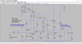
The stand out features are,
1 The input stage uses a very odd darlington arrangement on the inverting input side. Truly bizarre.
2/ The tail current for the LTP relies on a resistor, no CCS here.
3/ The collector loads for the LTP are totally unbalanced at DC, and at AC, one side is decoupled to ground.
4/ The top end of the feedback resistor is partially coupled via a large cap to the non inverting input, as also is R3.
5/ There is a slow start circuit at the top left to minimise thumps on power on.
6/ The VAS current is low at around 2ma.
7/ A PNP device is used for the VAS and this allows the intriguing prospect of bootstrapping via the speaker output coupling cap. The downside of this is that the 2ma VAS current flows in the speaker with R13 catering for when no load is attached.
8/ The output devices (TIP3055 in the original) have no emitter resistors and I do recall this amp being my first introduction to 'thermal runaway' as I watched my AVO8 meter needle rapidly climb.
9/ The zobel network values are correct according to the published diagram. I can't recall there being a correction made to these at a later date.
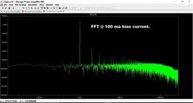
So I thought it might be fun to simulate this old timer and present the results here. The original used BC109C for the input stage and BFY56/BC461 for the drivers. The details in the magazine gave no insight whatever into the design other than how to adjust the bias and midpoint voltage. The distortion at 1 watt/8 ohms is around 0.08% but the FFT at this level shows a 'nice' structure.
So was it an inspired design ? or just another also ran from an era that gave us the like of the Texan and numerous other offerings.
I began taking magazines such as Practical Wireless, and it was here some 40 years ago that a diy project captured my imagination and so I had a go at building it. I was able to etch boards by this stage and so I followed the basic layout given in the magazine.
The amplifier was the 'Practical Wireless Europa' and now, many many years later I stumbled on the magazine as a download from the American Radio History: Documenting the History of Radio TV and FM broadcasting site.
I remember the amp as always being very engaging to listen to and so I thought I would look a little more closely at the design. Its a curious circuit from a designer I've never heard of before or since...
The stand out features are,
1 The input stage uses a very odd darlington arrangement on the inverting input side. Truly bizarre.
2/ The tail current for the LTP relies on a resistor, no CCS here.
3/ The collector loads for the LTP are totally unbalanced at DC, and at AC, one side is decoupled to ground.
4/ The top end of the feedback resistor is partially coupled via a large cap to the non inverting input, as also is R3.
5/ There is a slow start circuit at the top left to minimise thumps on power on.
6/ The VAS current is low at around 2ma.
7/ A PNP device is used for the VAS and this allows the intriguing prospect of bootstrapping via the speaker output coupling cap. The downside of this is that the 2ma VAS current flows in the speaker with R13 catering for when no load is attached.
8/ The output devices (TIP3055 in the original) have no emitter resistors and I do recall this amp being my first introduction to 'thermal runaway' as I watched my AVO8 meter needle rapidly climb.
9/ The zobel network values are correct according to the published diagram. I can't recall there being a correction made to these at a later date.
So I thought it might be fun to simulate this old timer and present the results here. The original used BC109C for the input stage and BFY56/BC461 for the drivers. The details in the magazine gave no insight whatever into the design other than how to adjust the bias and midpoint voltage. The distortion at 1 watt/8 ohms is around 0.08% but the FFT at this level shows a 'nice' structure.
So was it an inspired design ? or just another also ran from an era that gave us the like of the Texan and numerous other offerings.
Attachments
Plenty of quirks as you mention, though some of them may be explained by the designer coming from the world of germaniums. Not super low-noise with the Darlington in the feedback, I reckon. The designer sure liked his bootstraps though (that's what C2 is for, the other is the one around the output stage like I've seen in some Grundig portable radios of the time). Makes sense with so little VAS current though.
Doesn't look safe for headphones.
Hint: The <Ctrl>-<G>rid makes things easier to see.
Doesn't look safe for headphones.
Hint: The <Ctrl>-<G>rid makes things easier to see.
The designer was a Mr C Toms B.S.C. (well I assume it was a Mr) and I've never seen anything of his work other than this. You are correct about the noise aspect although I never really noticed it at the time. A 220k feedback resistor as well. It was a cracking power amp though back in the day.
TaHint: The <Ctrl>-<G>rid makes things easier to see.
Interesting to see a long tailed pair input on a single supply capacitor output amp. However weird this one is with the darlington. Apex AX6, Armstrong 621, Leak Delta70, DynacoST120, Basic50 , maona 5555, TGM8, all use emitter resistor feedback on the input. Only m2rac repaired 2n3773 amp (a commercial design origin not named) and Panasonic SU380 use LTP. I'm a bit interested in the darlington, I need >100k input resistance for compatibility with a PAS2 preamp and only ST120 has it, due to special input transistors BC108C no longer stocked for sale.
The no output emitter resistors probably comes from the RCA 2n3055/40636/39250 not needing them due to internal resistance. The TI TIP3055 surely did.
The no output emitter resistors probably comes from the RCA 2n3055/40636/39250 not needing them due to internal resistance. The TI TIP3055 surely did.
Last edited:
Hi indianajo,
-Chris
Check any J-FET input power amplifier. You can change the resistors from gate to ground without running into many problems if it's only 100K or thereabouts you need. The ST-120 isn't known for how smooth sounding it is.I need >100k input resistance for compatibility with a PAS2 preamp and only ST120 has it, due to special input transistors BC108C no longer stocked for sale.
-Chris
Hi Mooly.
" 3/ The collector loads for the LTP are totally unbalanced" (R7 - R8).
In this respect it resembles the Naim NAP140. The desbance of R collectors. The famous and disowned R 22K. It is said to produce distortion in the 2nd harmonic. This can be a secret.
Another secret will be the Q3 transistor? That benefit is in LTP?
Something else that contributes to increased 2nd harmonic distortion is the quasi output stage. Something else that contributes to the increase of the 2nd harmonic distortion is the quasi output stage. It is also the bootstrap with different values of resistors R12 - R13.
This is what I can say from my limited knowledge.
It is a mysterious circuit? I wonder: will other secrets?
Regards
Attachments
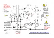
Thanks, that is interesting. I've a vague recollection that the Europa specified a tant for the feedback cap, and I see your diagram also mentions a tant is best. You wonder... you really do wonder where and how these designs originate and how ideas filter down.
The bootstrap is unusual because as soon as the speaker is connected, R13 is effectively shorted out.
The bootstrap is unusual because as soon as the speaker is connected, R13 is effectively shorted out.
C7 is something I think Doug Self refers to as 'shunt lag' compensation, it's simply a cap across the VAS stage and is nowadays regarded as a poor solution. If you imagine an HF signal at the collector of the VAS, then the VAS stage has to drive the reactance of that cap as a load. Not good.
No Re was (is) a serious omission imo and as I mentioned, this amp gave me my first real taste of what is meant by thermal runaway. Q3 I have no idea on. It looks unlikely but it worked well subjectively.
R2 is simply part of the resistive divider that allows the midpoint volts to be set but it is also a point that allows feedback to be introduced via C2. The top of R11 sees essentially the same AC voltage as the main amplifier input... the two inputs of an opamp if you like, inverting and non-inverting. By feeding that signal onto R2 and the DC bias preset we get a bootstrap action that effectively raises the input impedance of the amplifier.
C5 removes all AC from the collector of Q2/Q3. If that wasn't done then the distortion would rise several times over. Q2/Q3 collector is used for DC feedback only for the bias trimmer.
Q4 and Q5 are a simple slow start. The voltage on the base of Q4 will rise exponentially-ish at power on, the transistors simply being the equivalent of a series pass 'regulator' allowing current to be drawn from the emitter of Q5. Q5 emitter follows the voltage on the 100uF cap.
Good 'innit
I wonder if the slow start action of Q4 and Q5 would translate to a split-rail amplifier design and just how effective it might prove to be. It looks easy enough and perhaps using an SMD Darlington like BCV 27 could be a cheap, tidy solution in some cases of switch-on thumps where a relay isn't warranted 
I'll take a relay any time over this.
No doubt on that score. Nowadays equipment should be 100% silent at both power on and power off. There is just no excuse for it to be any other way.
Duhh...yes, I should have considered polarityremember this design is using NPN differential for inputs and a PNP VAS
That could mean using some unusual parts like BCV46, BC636 etc or just reverting to simple transistors as shown.I would have thought that the input pair could still "snap" on at some point as the supply voltage increased. This is what I assume I heard even when using a variac to gingerly power up typical AB power amplifiers, though I guess the sequence of junction turn-ons and resulting pulse peaks varies a lot between the countless designs and their various rise times.
It may be a difficult question now but do you recall if your Europa amplifier was near enough to silent at power-up/down?
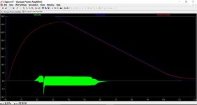
OK, so here is the output voltage as the supply rises and falls at power on/off. 'Vslow start' is also shown which is the emitter volts of Q5. The input signal was that needed to produce 2.83vrms at the output. Switch off is very well behaved. A little glitch at power on.
Attachments
Thanks Mooly, those time constants could be worked on if need be. I haven't found the PW issue in which the Europa article appears but I did see 'Mr' Toms had some influence at PW and is credited as a consultant from F.K. Electronics, whoever they were. He also contributed to another variation on that design with slow start, and odd Darlington LTP at page 674 here: http://americanradiohistory.com/Archive-Practical/Wireless/70s/PW-1975-12.pdf.
Perhaps that design was more popular than we might imagine and must have been a hit at the time.
Perhaps that design was more popular than we might imagine and must have been a hit at the time.
- Status
- This old topic is closed. If you want to reopen this topic, contact a moderator using the "Report Post" button.
- Home
- Amplifiers
- Solid State
- Revisiting an old 1970's design. Was it inspired, or just an 'also ran'.