Hi everyone,
some years ago I purchased an Amadeus Gold designed and manufactured by sondex ltd in the uk. It was blown up at one of the childrens parties and got boxed in the workshop years ago for later repair. My grandaughter just had her 16th so I thought it fun to resurrect the amp her mum had blown up.
I am not an audiophile by any stretch but I think I can recognise quality. I do have very good practical skills and passable theoretical knowledge, although linear circuits have not previously been my main interest, I thought this would be fun to repair and I would benefit from learning. Maybe somebody would like to see the design, and maybe advise me as to how I might be able to set it up as the designer intended.
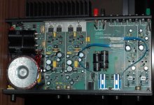
In the first Instance I will try to post a raw pic of the amp itself.
lets see what happens...................... lets see if I can upload a pic
...... first lesson... do not try to view thumbnail in preview mode firefox will not let you go back and the whole post is lost!!!!!
cheers
..
some years ago I purchased an Amadeus Gold designed and manufactured by sondex ltd in the uk. It was blown up at one of the childrens parties and got boxed in the workshop years ago for later repair. My grandaughter just had her 16th so I thought it fun to resurrect the amp her mum had blown up.
I am not an audiophile by any stretch but I think I can recognise quality. I do have very good practical skills and passable theoretical knowledge, although linear circuits have not previously been my main interest, I thought this would be fun to repair and I would benefit from learning. Maybe somebody would like to see the design, and maybe advise me as to how I might be able to set it up as the designer intended.
In the first Instance I will try to post a raw pic of the amp itself.
lets see what happens...................... lets see if I can upload a pic
...... first lesson... do not try to view thumbnail in preview mode firefox will not let you go back and the whole post is lost!!!!!
cheers
..
Attachments
99% of faults will be failed output transistors (on the heatsink) and probably the driver transistors too. Low value resistors can get taken out too when devices fail.
If you had a circuit we could advise much better but it looks a classic and straightforward design.
Too late in the day to "get heavy" but a start would be checks on the output devices to see if any read short circuit.
If and when it gets powered up the advice is always use a bulb tester to save damage and mishaps.
Two threads here will give you insight into what is involved,
http://www.diyaudio.com/forums/solid-state/121748-arcam-alpha-3-left-channel-broken.html
http://www.diyaudio.com/forums/solid-state/233880-help-repairing-pioneer-m3.html
hi Mooly,
Actually I too am a little tired today....
History is that I replaced the TIP3*c pairs and two of the bd140 drivers, a couple of resistors were out of 1% range so they were replaced and have replaced some pots that were also degraded.
The amp is working but I would like to understand a little better what is going on .
Classic design but layout with letraset and the resist pen (those were the days)
First off I mapped part of the the board layout straight into cadsoft and then reverse created a schematic and have been fiddling with the nets to make sense of what you correctly say is fairly classic and straightforward design. ( not my department though )
I am having difficulty exporting cadsoft eagle layout and schematic into a form that I can post. It is difficult to make the feedback loop make readable sense in the schematic.
thanks for interest, will read your links
cheers
..
The "style" of that looks very like my old Cambridge C70, the capacitors, switches, pcb silkscreen etc
Any non standard files can be put in a zipped folder and attached. (I don't use Eagle 🙂)
One thing that stands out in the picture of the amp is the (apparent) lack of thermal sensing of the output stage which in 99% of amps is a transistor in thermal contact with the heatsink, what is called the Vbe multiplier. Thermal stability and possibility of thermal runaway is a real danger.
One thing that stands out in the picture of the amp is the (apparent) lack of thermal sensing of the output stage which in 99% of amps is a transistor in thermal contact with the heatsink, what is called the Vbe multiplier. Thermal stability and possibility of thermal runaway is a real danger.
Thanks David, I believe that there does seem to be similarity between some of the designs that I have come across under "vintage" especially the stock components, the remote selector for example, seen as the blue ribbon that has a steel insert which slides. A first glance it reminded me of a grounding strap. I did have to disassemble the switch assembly and clean the contacts which had tarnished/oxidised, as two of the inputs were inactive. I will have to service the selector for the preamp output at a later time. I chose not to put it in the sonic tank but did it by hand with cotton buds and finally cleaned up with isoprop and safe low residue solvent. I try to be as careful as possible with all solvents, a slow and inevitable destruction to any component is the dreaded WD40.
hi Mooly,
I was hoping to be able to post in a format that was easy and convenient for the forum to read, I do not mind spending a little time getting them converted. On that subject I have tried to trace the current owners of the design and have emailed Woodside Electronics who I believe inherited all designs from sondex and Radford(mainly tube amp bods), I have not had any replies, I was respectfully asking permission to publish the design. I can only assume that nobody holds the rights, but I would have preferred as a courtesy.
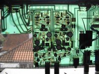
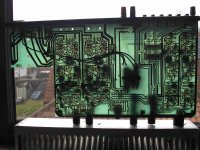
I have two silhouetted photo images taken of the front and back (mirrored) of the pcb which I used to copy the layout.
Thanks for explanation of the Vbe multiplier module, I replaced both BD140 with as best matching hfe as possible the BD139Y had a BC182 mated back to back, again I remounted balanced replacements taking care to mate the surfaces correctly, added a bit of thermal compound and rubber booted. I am assuming this might be the thermal protection module to which you referred.
cheers
..
hi Mooly,
I was hoping to be able to post in a format that was easy and convenient for the forum to read, I do not mind spending a little time getting them converted. On that subject I have tried to trace the current owners of the design and have emailed Woodside Electronics who I believe inherited all designs from sondex and Radford(mainly tube amp bods), I have not had any replies, I was respectfully asking permission to publish the design. I can only assume that nobody holds the rights, but I would have preferred as a courtesy.
I have two silhouetted photo images taken of the front and back (mirrored) of the pcb which I used to copy the layout.
Thanks for explanation of the Vbe multiplier module, I replaced both BD140 with as best matching hfe as possible the BD139Y had a BC182 mated back to back, again I remounted balanced replacements taking care to mate the surfaces correctly, added a bit of thermal compound and rubber booted. I am assuming this might be the thermal protection module to which you referred.
cheers
..
I think I see what you refer to re the BD's and the BC182 in contact. Very unusual.
If you have a schematic in Eagle then something like Windows snipping tool (Vista and W7) would make a .jpg from whatever is displaying on screen.
If you have a schematic in Eagle then something like Windows snipping tool (Vista and W7) would make a .jpg from whatever is displaying on screen.
It should be fairly straightforward to sketch the circuit itself, certainly for the main power amps.
Looking at the outline, the power transistor emitters appear to go to the rails so its going to be a CFP (complementary feedback pair) configuration.
Looking at the outline, the power transistor emitters appear to go to the rails so its going to be a CFP (complementary feedback pair) configuration.
Hopefully this is partially readable, I am concerned that I do not seem to be able to get the file small enough to maintain readability, The reason all the components are well spaced is that I keep rearranging to try to make sense of the design..
anyway here is a possible interpretation of the power amp section.
also included specification from the original manual
cheers
..
anyway here is a possible interpretation of the power amp section.
also included specification from the original manual
cheers
..
Attachments

Truly sorry for wasting forum storage, I am really struggling here to get a decent image exported out of Cadsoft. Am going to shift over to windows OS. Cadsoft are geared up to export images etc etc for use as litho, not 100k to post on a forum.
I will not be defeated, just de-stress, and plan a different approach.
Are you able to delete the failed attachment?
cheers
..
I will not be defeated, just de-stress, and plan a different approach.
Are you able to delete the failed attachment?
cheers
..
problem solved.. the origin had accidentally been relocated. I also realised the schematic and layout are inconsistent so there is still quite a lot to do.
also I have just realised there are limited values in the schematic, hopefully for the moment they are obvious to experienced. Components in odd locations means I have not quite yet grasped their purpose.
thanks for deleting the bad upload. And thanks for taking time to read my posts
cheers
..
also I have just realised there are limited values in the schematic, hopefully for the moment they are obvious to experienced. Components in odd locations means I have not quite yet grasped their purpose.
thanks for deleting the bad upload. And thanks for taking time to read my posts
cheers
..
Attachments
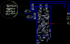
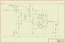
The thermal sensing point is correct as the output stage is a CFP. The Vbe changes of the power devices is not important. I think you have the wrong part in the thermal sense, it should be the Vbe multiplier TR9. TR10 is output protection
The CFP stage will run at low bias current that's dependent on the value of R49/50, probably in the range of 8 to 12 milliamps. The other preset adjusts the output voltage to approx half the rail voltage to allow equal swing either way.
thanks for help,
I would like to try and lay out the schematic in a form that shows groups as individual modules, output stage, bias, vbe, output protection, signal conditioning,
I have done some rearranging, but I now need to do some reading up. I know the schematic is a valid design, I know it is also made up from probably standard tried and tested modules, It is just a question of identifying which exact modules have been used in this design and arranging the components in the schema.
cheers
..
Attachments

TR8 is known as the VAS or voltage amplifier stage.
R35 and R37 are the main "feedback" network and the ratio of these sets the voltage gain... in principle... without seeing the exact circuit and values there's some input from R36 and the smaller value caps (compensation).
Its a single ended input stage (good for sound quality because the distortion is predominantly even harmonic)
TR10 and 11 are the protection circuit and work by sensing volt drop across the low value output resistors. I don't think the circuitry is drawn quite correctly around there 🙂
The emitter of TR9 seems to be missing a resistive return to ground.
The emitter of TR9 seems to be missing a resistive return to ground.
R36, R37 and C22 form a boot-strapped resistor load. A simple resistor to ground would make this a very low open-loop gain design.
Last edited:
- Status
- Not open for further replies.
- Home
- Amplifiers
- Solid State
- Reverse engineering a John Widgery Sondex/Radford SS amplifier.