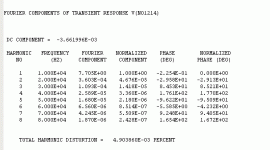
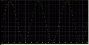
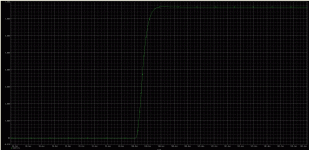
I have had some peeves with the classic Hitachi Lateral mosfet amplifer designs from the app notes in the early 80's, mainly due to the limited amount of current available from the 2nd differential stage for charging the gates of the output lateral mosfets. I sorta had my way with the original design and came up with one utilizing a Pmos input, bipolar second differential stage, and a follower stage to drive the output lateral fets. Since I don't have lateral fets in my PSpice bag of tricks, I used a Vgs multiplier for bias and a complementary vertical fet output stage. In practice, I would use a simple resistive bias scheme and lateral outputs (Exicon, anyone?). Attached are a preliminary schematic, output, and sim distortion profile.
Attachments


I just nabbed a stash of the nice Toshiba TO-126 160V driver bjts. I'm thinking that's what I'll use in the second differential stage, as the capacitance is smaller than the Fairchild KSA/KSC bjts I also have on hand. Another possible option would be 2SA965/2SC2235 TO-92L devices (also Toshiba) I may also try a tiny bit of degeneration on the second diff stage to see how that plays out in simulation (linearity vs. raw open loop gain).
In practice, I would implement the current sources shown in the simulation with my favorite depletion mode mosfet, the BSS159, perhaps with a series resistor to soak up extra voltage that would cause excess power dissipation (perhaps not needed on the 2nd diff stage).
In practice, I would implement the current sources shown in the simulation with my favorite depletion mode mosfet, the BSS159, perhaps with a series resistor to soak up extra voltage that would cause excess power dissipation (perhaps not needed on the 2nd diff stage).
Last edited:
I won't, forget the protection, though I will do protection my own way to minimize the capacitance hanging of the input.
Layout is almost done, though I need to go in and check that I got the right polarity for the hookup of the 2nd diff amp. I originally messed this up in the sim and the output kept slamming to one rail - duh...
I'm just going to throw this out there, since you're using a pmos input, what about this little guy (LP0701). It has a fairly low max VDS so would require cascoding. But it would probably be the only amp in existence with lateral FETs on the input and output. Which doesn't really mean anything but it sounds cool 😎 Admittedly, I don't really know what I'm doing, but I play around in Spice. I managed to find a shared library with many audio parts, including the Exicon FETS. So here you go. I attached the model for LP0701 too, just in case you're feeling froggy 😛
Attachments
I'll likely end up using the Zetex/Diodes Inc. enhancement parts, as I have ~500 of them and the E-line package makes it easy to glue matched fets together. I usually use JB Weld/JB Kwick for bonding, as it has a metal filler that enhances the thermal coupling. - not quite as nifty as Arctic Silver, but the thermal resistance between devices will still be better than thermal resistance to ambient, and that's what counts.
BTW - sho' nuff, I had the inputs to the 2nd diff amp crossed up in my layout - fixed now, without even a lot of roaring and screaming.....
might be interesting, but it has a lot of capacitance for an input device.I'm just going to throw this out there, since you're using a pmos input, what about this little guy (LP0701). It has a fairly low max VDS so would require cascoding. But it would probably be the only amp in existence with lateral FETs on the input and output. Which doesn't really mean anything but it sounds cool 😎...
Right now, my layout has space for only one output device , top and bottom. I may end up using some dual-die Exicons I scored on Ebay, or just bite the bullet and squeeze in a second set of output devices and source resistors.
I'm a bit curious about the shown feedback network (R16, R17, C2, R7) in conjunction with the input filter (C1, R18).
This input filter has a turnover frequency of 3Hz (a zero) but the feedback has a serious rise of amplification between 0.1 to 10Hz (two poles C2-R16//17, C2-R7). If this feedback network is configured to keep the overal response flat down to 1Hz at least (to counter the zero at 3Hz), why this risk for thermal instability or near dc instability?
I have to make some plots to clearify, but for now, has this amplifier 'from the app notes in the early 80's' ever been build by Hitachi?
I've never seen such a feedback network before, so what is the idea behind it?
That particular feedback scheme has been used as a default solution by me since the late 70's. I first came across it in an analysis of a Nakamichi amplifier circuit in Audio magazine circa 1978 or so. It implements unity gain DC feedback to avoid amplifying input offset, and takes a nasty electrolytic out of the feedback loop. That feedback method is also shown in Horowtitz and Hill's "Art of Electronics". Using jfets or mosfets for the input differential stage allows use of a high value for the unity gain feedback resistor, and consequently a reasonable value for the coupling capacitor. I use a 2u2 polycarbonate or polypropylene cap, whichever I can gets my hands on. Calculating the transfer function for that feedback scheme is an interesting exercise (it's not immediately obvious), especially if you load it into Excel and graph it out.
BTW, I always use a coupling cap at the input of my amplifiers, as I don't trust what the cold, cruel world has to offer regarding DC offset on signal outputs.
BTW, I always use a coupling cap at the input of my amplifiers, as I don't trust what the cold, cruel world has to offer regarding DC offset on signal outputs.
Last edited:
Ah! From Nakamichi! Yes, agreed, that ecap to block dc, after some years problems arise. I prefer there (if in need) a nonpolar ecap (twice the supply voltage) anyhow as dc there is in stable condition low but during switching on and off unknown, uncertain or of surprising value. I use Spice for analysis, and there the bode plot (thus both amplitude and phase) gives a clue about the transfer already.
What page in H&H?
Just to avoid discharge of C1 (V3 side) when something is connected to it in the real world, a resistor (100k) would prevent that (R18 also 100k).
What page in H&H?
Just to avoid discharge of C1 (V3 side) when something is connected to it in the real world, a resistor (100k) would prevent that (R18 also 100k).
Alas I don't have that one - can you post the original figure for educational purposes?
Much appreciated!
I'll try to post the bode plots soon.
Much appreciated!
I'll try to post the bode plots soon.
- Home
- Amplifiers
- Solid State
- Retool of Classic Hitachi App Note Lateral FET Amplifier