Perhaps John Curl's Blowtorch preamplifier part III post #32,387 can help you.Alas I don't have that one - can you post the original figure for educational purposes?
I've been tearing up the layout to add extra power devices, so the board will have a theoretical 100W capability. Somehow I don't really trust the double-die Exicon devices, and would prefer a design where I can apply a gate stopper to each device.
I don’t know about whether to trust the double-die devices or not, but I’m happy with your decision, because I have a small batch of K135/J50 pairs idling for a new design. 
I have a small stash of the old Hitachi TO-3 devices, a couple of tubes of the Semelab BUZ TO-3s, and a small number of the Hitachi/Renesas TO-3P devices. I actually got the P-channel TO-3Ps from Electronic Goldmine a few years ago - I'll have to test them to see if the source pin is in the center like it should be. For that matter, I'll also need to retool the layout as well to make it so. It might make life a little easier for me.
Last edited:
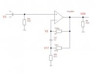
Possibility of separating supply of the output laterals would probably be desired. As it is the design can output 28-30 Vp, while the laterals would dissipate ~70-84W more than needed at peaks.
Right now, I'm separating the supplies for the driver stage and the output stage to make a boost supply possible.
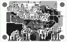
I finally got my lateral fets and PCBs on Thursday, no thanks to DHL. I had to drag my skanky behind to a DHL depot for manual pickup, as DHL coulldn't get it together enough to show up for delivery when my work premises were actually open. I'm slowly populating two of the amplifier boards I received. How I actually stuff the boards will be determined by the gate-source voltages of the output fets I'll be matching.
Like everything else, it's being multiplexed with a stack of other projects, a paying job, and a volunteer DJ gig at a nearby college radio station. I have projects stacked to the moon. and must work on them with begged, borrowed and stolen time. I couldn't precisely tell you where the boards in question are even located these days. As usual, the hardest part will be fitting up the amp with box, power supply, and heat sinks.

- Home
- Amplifiers
- Solid State
- Retool of Classic Hitachi App Note Lateral FET Amplifier