I am looking at the output of the amplifier, and it oscillates at a frequency that depends on the rail voltage. I think this is due to relaxation oscillations rather than resonant oscillations. Would this be the case, and what causes relaxation oscillations in an amplifier? The frequency is on the order of hundreds of kHz, with the frequency increasing with rail voltage, and it has a very irregular impulsive shape to it.
Your chances of getting a useful answer would increase considerably if you posted a schematic.
Parasitic oscillations always depend on the supply voltage to some extent.
If the waveforms are irregular, the amplifier could be oscillating chaotically. Without input signal, you need three orders and a strong nonlinearity for that.
Does it always oscillate or can you kickstart or kickstop the oscillations by driving the amplifier into clipping?
One way to get relaxation oscillations is to unintendedly make a Schmitt trigger with a slow feedback loop around it.
Have you thought about what happens when transistors saturate? Are there any common emitter stages with emitter degeneration that change polarity when driven in saturation? Any base rails that collapse when a current source on the rail saturates?
Another way to get relaxation oscillations is to use transistors above their VCEO rating; avalanche breakthrough with a shunt capacitor makes the solid-state equivalent of the good old neon lamp oscillator.
I forgot to ask the most obvious questions: during the design phase, how did you analyse the stability of any feedback loops? Do any of them have more than two dominant poles? (Loops with more than two dominant poles can be stable, but they have the reputation of bursting into oscillations when overdriven, although not all of them do so and if they do, it can usually be solved by clamping internal nodes.)
The oscillations reliably start once the variac voltage exceeds a certain value without fail. Current consumption will also greatly increase at the same time. They will continue even if the variac voltage is decreased below the voltage at which oscillations start, until the rail voltages decreases to a very low level. The oscillation waveform is not chaotic, it has a regular period, but this period depends on the voltage, and the output voltage is high asymmetrical.
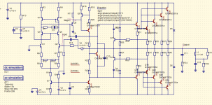
The following the C300 amplifier schematic that I am using. I modified it by adding faster VAS and output transistors (3281/1302 with fT=30 MHz), and I'm trying to rebalance the feedback to prevent oscillation. I am using faster transistors to try to decrease the distortion by increasing the loop bandwidth.
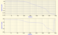
The original design has two pole compensation, one with the standard Miller compensation (C9) and the section with R5/C3 in the LTP. Originally, the circuit used slow output transistors (fT=4 MHz) and slow VAS transistors (MJE340/350). I wanted to try to get away with a single pole compensation so I changed C9 to 150 pF. I modeled the open loop bandwidth and the phase margin (according to simulation) is on the order of 80 degrees, with unity gain occuring about 200 kHz.
I could try to add the second pole of compensation, for example R5=620 ohm, and C3=100 pF, but this seems to me to be papering over the problem. If the phase margin is decreasing below zero, I would like to know why. If it isn't because of this, I am trying to figure out what other mechanisms for oscillation there could be.
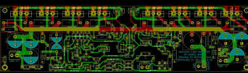
The layout is also included. Most of the top layer (except where the power transistors are) is a solid ground plane with holes through it for the plated-through holes. The output is kept away from the input by being on the opposite side of the board (input at bottom, output at top), and the output is taken off to the side. I would think parasitic capacitance and inductance between traces would be relatively low.
Sorry for the excessive information but I have found that to get interest and help I have to be careful to provide enough information so that my problem can be investigated but not too much to so that others lose interest.
The following the C300 amplifier schematic that I am using. I modified it by adding faster VAS and output transistors (3281/1302 with fT=30 MHz), and I'm trying to rebalance the feedback to prevent oscillation. I am using faster transistors to try to decrease the distortion by increasing the loop bandwidth.
The original design has two pole compensation, one with the standard Miller compensation (C9) and the section with R5/C3 in the LTP. Originally, the circuit used slow output transistors (fT=4 MHz) and slow VAS transistors (MJE340/350). I wanted to try to get away with a single pole compensation so I changed C9 to 150 pF. I modeled the open loop bandwidth and the phase margin (according to simulation) is on the order of 80 degrees, with unity gain occuring about 200 kHz.
I could try to add the second pole of compensation, for example R5=620 ohm, and C3=100 pF, but this seems to me to be papering over the problem. If the phase margin is decreasing below zero, I would like to know why. If it isn't because of this, I am trying to figure out what other mechanisms for oscillation there could be.
The layout is also included. Most of the top layer (except where the power transistors are) is a solid ground plane with holes through it for the plated-through holes. The output is kept away from the input by being on the opposite side of the board (input at bottom, output at top), and the output is taken off to the side. I would think parasitic capacitance and inductance between traces would be relatively low.
Sorry for the excessive information but I have found that to get interest and help I have to be careful to provide enough information so that my problem can be investigated but not too much to so that others lose interest.
Attachments
It starts when you slowly ramp up the supply. Have you tried slowly ramping up the supply in a transient simulation?
There are two ideal bias voltage sources in the schematic, V2 and V3. These must be something else in reality. Is the voltage across whatever is used in real life constant during the oscillations?
There are two ideal bias voltage sources in the schematic, V2 and V3. These must be something else in reality. Is the voltage across whatever is used in real life constant during the oscillations?
Last edited:
No, I haven't figured out how to do that yet, but it's a good suggestion. It will be a relatively long simulation as it has to be over a second, but simulated at the microsecond scale.
When you do it without input signal, the simulator will automatically take small steps when there is a lot happening and large ones when there is not. So basically when the simulation becomes slow, you know it's oscillating.
By the way, the integration method may affect transient simulation results. The trapezium integration method has no numerical damping, but it causes artefacts on the current waveforms. Second-order Gear has no such artefacts, but has numerical damping.
By the way, the integration method may affect transient simulation results. The trapezium integration method has no numerical damping, but it causes artefacts on the current waveforms. Second-order Gear has no such artefacts, but has numerical damping.
You inject the input signal on the inverting input Q2 with or without input resistor? And there is this grounding resistor R15 as if the input on Q2 is the feedback node of an non inverting amp with input on Q1.
If oscillation is supply dependent, the open loop amplification is... or can be also supply dependent.
Which stage changes in open loop amplification when changing the supply?
You can simulate this with separate stages, but given the current sources you may find no result here.
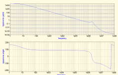
The open loop peak at 1.1MHz is a good candidate at Ao=0.4. What is creating this pole?
What are the values of R5-C3 and C9? C9 interacts with Ccb of Q10 (no frequency fixing Rc-load here).
If oscillation is supply dependent, the open loop amplification is... or can be also supply dependent.
Which stage changes in open loop amplification when changing the supply?
You can simulate this with separate stages, but given the current sources you may find no result here.
The open loop peak at 1.1MHz is a good candidate at Ao=0.4. What is creating this pole?
What are the values of R5-C3 and C9? C9 interacts with Ccb of Q10 (no frequency fixing Rc-load here).
1/ Try increasing C9 a little.
2/ You have drivers going straight into outputs, try a 10R in series to base of each output.
2/ You have drivers going straight into outputs, try a 10R in series to base of each output.
I am only injecting the signal at Q2 to estimate the open loop gain. I am following what is being done in this presentation:
Output L_1
In this presentation on slide 3, it shows how to modify the circuit to estimate the open loop gain, while I have tried to follow. I tested the method with the circuit in the presentation and got the same results so I assumed it worked. In the real circuit, the input is grounded and injected at Q1.
Currently, I leave C3=0 pF because I am trying to avoid using a second pole of compensation. The original design calls for C3=220 pF. C9 is currently 150 pF, where the original design called for 33 pF, but I increased it because the simulations showed the increased open-loop bandwidth required a larger Miller capacitor. Unfortunately, MJE15033 has no spec for Ccb or output capacitance. Perhaps MJE15032/MJE15033 is a poor choice for VAS because it has too much capacitance? It was one of the goals of my design to come up with a simplified design. I was replacing the MJE340/350 in this role.
I also changed BC546C/BC556C for 2N5551/2N5401. Could this be a problem? I felt uncomfortable using transistors not rated for the full supply voltage.
You inject the input signal on the inverting input Q2 with or without input resistor? And there is this grounding resistor R15 as if the input on Q2 is the feedback node of an non inverting amp with input on Q1.
If oscillation is supply dependent, the open loop amplification is... or can be also supply dependent.
Which stage changes in open loop amplification when changing the supply?
You can simulate this with separate stages, but given the current sources you may find no result here.
The open loop peak at 1.1MHz is a good candidate at Ao=0.4. What is creating this pole?
What are the values of R5-C3 and C9? C9 interacts with Ccb of Q10 (no frequency fixing Rc-load here).
Please disregard the message, I misread what you said, I apologize...
By the way, would not using base stopper resistors cause this problem? I am using larger than usual emitter resistors (0.39 ohms) but this is not quite the same thing, but should help share current more evenly. The reason I am asking is that I would like to avoid a respin of the board if possible and adding a large base stopper resistor for every transistor would probably require that.
By the way, would not using base stopper resistors cause this problem? I am using larger than usual emitter resistors (0.39 ohms) but this is not quite the same thing, but should help share current more evenly. The reason I am asking is that I would like to avoid a respin of the board if possible and adding a large base stopper resistor for every transistor would probably require that.
Attachments

I had a similar amp design.
Increasing VAS cap didnt help much.
Fix was putting base stoppers resistors in output bases.
Increasing VAS cap didnt help much.
Fix was putting base stoppers resistors in output bases.
In your post #15 the peak at 1.1Mhz has almost disappeared, so that's what will surpress unwanted oscillations. Compare this commercial circuits from the Sony Esprit series (eighties). Left is the phone pre with active riaa but with a RC in the front stage, right a flat amp with a feedback cap only. Both stages has an enormous open loop gain (>80dB).
Attachments

Last edited:
- Home
- Amplifiers
- Solid State
- Relaxation oscillations in an amplifier