At this point I feel like it is mostly about fine tuning performance at 20kHz.
Comes down to finding balance between nice clipping behavior and low THD20 rating.
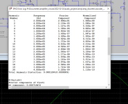
Reducing LTP degeneration resistors to 82R gives lower THD20. I tried reducing down to 47R but that is where it is breaking into oscillation.
Bootstrapping VAS cascode aids in negative clipping behavior.
THD20 reduced to 0.000128% as a result.
THD1 stays at 0.000009 just like before.
Comes down to finding balance between nice clipping behavior and low THD20 rating.
Reducing LTP degeneration resistors to 82R gives lower THD20. I tried reducing down to 47R but that is where it is breaking into oscillation.
Bootstrapping VAS cascode aids in negative clipping behavior.
THD20 reduced to 0.000128% as a result.
THD1 stays at 0.000009 just like before.
Attachments

These are really nice THD numbers!Just so you have a baseline,
These are the Wolverine's sim numbers at 80w output into 8 ohms
0.000001% at 1k
0.000067% at 20k
I am just learning as I go right now, pretty new to simulators, but they are a lot of fun!
Changed supply voltage to 64V.
Changed load to 8 ohms.
Changed input A to 2.5V
THD20 is now 0.000056%
THD1 is back to 0.00001% 😭😂
Changed load to 8 ohms.
Changed input A to 2.5V
THD20 is now 0.000056%
THD1 is back to 0.00001% 😭😂
Attachments
Last edited:
That will be the next step. I have Cordell's book as reference it provides EF3 equivalent schematics with stray capacitances and inductances specified. Will be fun to tinker with those.included trace inductance and some output capacitance to ensure ef3 suitability
By the way, is it better to add cap multipliers comparing to beefing up CCSs? Meaning for PSRR?
Red led is less noise then zener
What you call OPL is LP (Loop Gain).
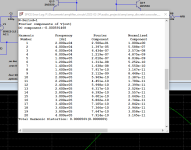
THD at 1kHz simulated is 0.000072% and at 20 kHz is 0.000110% for this conpensation method I used (OITPC). Be careful how you use TPC, revers the caps order.
Red LED is less noisier then zener. I don't see any advatage to bootstrap the each cascode independently.Looking nice! You are way ahead of me obviously in the amp design and simulator.
But the idea behind using two transistors were to bootstrap each cascode independently.
It can also be biased by just using zeners or LEDs.
I tested for clipping and it looks like adding booster cap around 150p to the BC junction of the CCS transistor helps to reduce oscillations.
Increasing cap to 470p completely gets rid of oscillations while clipping, but increases 20khz THD.
I replaced CCS transistor with another diode as it is more practical to use higher power dissipation transistor instead of dual SMD package like I planned before.
Your OPL looks really nice and flat! I wonder how did you get it?
Thank you for input!
What you call OPL is LP (Loop Gain).
THD at 1kHz simulated is 0.000072% and at 20 kHz is 0.000110% for this conpensation method I used (OITPC). Be careful how you use TPC, revers the caps order.
Keep the fire burning you are on a roll and its starting to look your not so much of a novice after all. You also seem to have fallen in luck with Dadod. Start looking for oscillations, adjust the compensation accordingly, each bjt adds about 30 degrees of phase shift or delay play around with the number of degrees and adjust compensation accordingly. Linear open loop gain up to 10k is usually not bad. Is there a thing as too much gain? How much gain is good enough that the output is not rusty and how much is too much that the amplifier is a loose canon. Remember feed back works a certain way. Feedback can even fail if the amplifier is unstable.
Fun continues!
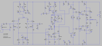
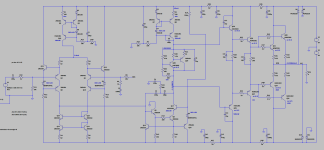
Cascoded Constant Current source supplies current to cascoded and bootstrapped Long Tailed Pair that is in turn loaded to the cascoded Current Mirror. Ah, the perfection!
Voltage amplification stage is beta enhanced and cascoded. Cascode is bootstrapped too! (I think if I implemented that correctly???)
VAS constant current source got cascoded as well!
Red LEDs everywhere!
Useful in a sense that they can help when debugging the actual board.
Vbe multiplier unfortunately cannot be cascoded and complimentary feedbacked instead...
Can EF3 OPS be cascoded? lol
On compensation:
Two pole compensation.
Increasing R15 (VAS E resistor) from 2.2k to 10k got rid of a peak in OLG around 1 to 10 Hz region.
Adding 220n cap to the ground removed second peak.
Clipping:
100p booster cap across VAS CCS BE helps to recover from positive clipping
Q15 in conjunction with R18 limits negative clipping
R14 helps to reduce excessive current applied to Q6 base.
Any comments?
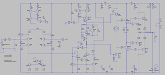
Attachments
Red LEDs everywhere!
What happens when light hits the amplifier?
You still cal it open loop gain (OLG), it is in fact loop gain(LG), means just value of available negative feed back.Fun continues!
Cascoded Constant Current source supplies current to cascoded and bootstrapped Long Tailed Pair that is in turn loaded to the cascoded Current Mirror. Ah, the perfection!
Voltage amplification stage is beta enhanced and cascoded. Cascode is bootstrapped too! (I think if I implemented that correctly???)
VAS constant current source got cascoded as well!
Red LEDs everywhere!
Useful in a sense that they can help when debugging the actual board.
Vbe multiplier unfortunately cannot be cascoded and complimentary feedbacked instead...
Can EF3 OPS be cascoded? lol
On compensation:
Two pole compensation.
Increasing R15 (VAS E resistor) from 2.2k to 10k got rid of a peak in OLG around 1 to 10 Hz region.
Adding 220n cap to the ground removed second peak.
Clipping:
100p booster cap across VAS CCS BE helps to recover from positive clipping
Q15 in conjunction with R18 limits negative clipping
R14 helps to reduce excessive current applied to Q6 base.
Any comments?
By the way, insert protection resistor betwen Q5 collector and the ground, it serves in case of cliiping to limit the collector current.
That's not the normal way to do a full Wilson current mirror: https://circuitdigest.com/tutorial/...ilson-and-widlar-current-mirroring-techniquesFun continues!
Cascoded Constant Current source supplies current to cascoded and bootstrapped Long Tailed Pair that is in turn loaded to the cascoded Current Mirror. Ah, the perfection!
Your version is more imbalanced than the original mirror you had.
I probed R4 and R5 with new CM:Your version is more imbalanced than the original mirror you had.
I(R4) = 2.0227059mA
I(R5) = 2.0227046mA
delta[] = 0.0000013mA
Here is the previous version with just a helper transistor:
I(R4) = 2.0414964mA
I(R5) = 2.0418133mA
delta[] = 0.0003169mA
Previous was not as many zeros..
Am I missing something?
What about just using better constant current sources? PSRR for positive supply should increase nicely..The cap multipliers reduce ripple and increase the PSRR of the stage.
You mean lightning?What happens when light hits the amplifier?
I suppose I could add some tesla coils to the VAS stage to use all of that energy to bootstrap my sound 😭 😂
A LED is to some extent a photodiode.ou mean lightning?
I suppose I could add some tesla coils to the VAS stage to use all of that energy to bootstrap my sound 😭 😂
For line level we are looking at between 0.316V to 2V across a 600ohm,2k or 10k resistor and wondering how to transform it to work on a 4 Ohm load, an inductive and capacitative load, reactive load.
1. We could use a transformer but now the voltage is useless. So we think; lets use a tube with its high voltage capability but not so much current capability to ramp up that voltage and then use a transformer to get the current up. Then we start thinking lets replace the tube and transformer with a SIT or why not multi stage tube amp? Using this approach the word feedback might even be a dirty word that might draw looks of disapproval.
2. Following from the first approach, your happy with your single fet class A amplifier but its not portable and eats up battery power really fast. On a bored weekend you remember the electronics 201 professor had mentioned comparators, timers and capacitors and you happened to have a couple of these left from that practical back in time. Immediately you get an eureka moment and after your done you don't care too much to listen to what you've just cobbled up but months down the line you demo your latest version of the design and there's interest. A couple years later the technology becomes mainstream in every portable.
3. Another approach, seeing that the voltage level lies at between 0.316V to 2V with max current flows of 200uA-500uA bjts would suit a bjt input stage running at low current so it acts as our voltage controlled current gain stage, we want to do as little voltage gain as possible here. We end up with a slightly beefier current and a slightly higher voltage. Our THD without feedback looks good, however if using feedback and aiming for lower THD a few rules can be Brocken but with caveats. A BJT is the most robust here. The next stage the VAS needs to perform magic, if we need to keep THD low this is where we do it. Operating a bjt here in current gain mode without feedback is erratic but with feedback yields lower THD depending on application a cascode maybe considered, plan B is to operate in voltage mode but that means a VAS with like 1000hFe,however with feedback a single lower hFe device can suffice. We can also choose to use a suitable FET for the VAS and run a warmer LTP current. If using feedback choices here dictate what you can get away in the input stage and vise versa. A resistor at the emitter or source provides the much needed linearity here especially if using no or low feedback, even if using feedback linearity doesn't hurt as it forces the device to be voltage driven which helps bring down that distortion. We can safely say this is the real amplifier. There's a reason some veterans become uptight once you start talking about ultra low 0.0000000%THD since stability and musicality become suspect(Yes ultra low distortion can be a dirty word sometimes).Now we need ourselves a current gain stage. If looking at FET outputs we need a driver that can deliver between 10mA to a couple hundred mA. BJTs beat FETs here in terms of THD, a reactive load also necessisates FETs to be included within the feedback loop. But for class A , FETs are safer but result in earlier clipping than BJTs. Implementation of the output stage matters. We can also start thinking how to lower distortion through parallelism. We could take feedback from the voltage gain VAS stage if the output is class A non FET or if a switching stage take the feedback after the output stage. We have more things to worry for example driving woofers and that is room treatment and bass decay, so we take the feedback after the output devices.
We can also learn something from power transmission, we keep power in the voltage domain and only go back to the current domain at customer premises. In a steady-state scenario, a higher current generally generates a stronger magnetic field compared to a higher voltage. Take time to build and listen to your designs.
Use headphones to listen to this demo https://www.diyaudio.com/community/threads/whats-good-enough.396039/#post-7307389
You don't need headphones listen to this feedback, hope it helps
For my case, I am looking at 4Vrms balanced signal that is coming from my DAC.For line level we are looking at between 0.316V to 2V across a 600ohm,2k or 10k resistor and wondering how to transform it to work on a 4 Ohm load, an inductive and capacitative load, reactive load.
That adds one more step in which signals will combine and everything else (noise or ground loops) will be canceled out.
And that is what I want my amp to amplify
Nice, now lets see that final design😉. You might also consider a no feedback design use a FET to ramp up that voltage gain then use BJTs emitter followers as outputs biased into class A for the first couple of watts to mask the switching, you may need to consider what VAS current and whether 2 stage or three stage emitter follower into four ohm gives you that warm sound, maybe stick to two stage for this one
Last edited:
- Home
- Amplifiers
- Solid State
- Reference discrete amplifier inspired by Wolverine and Cordell book