Hi all,
I am in the process of learning about amplifiers and have came up with a design that is closely resembles that of Wolverine.
I wonder what is the point of using cascodes for the IPS and so I omitted them.
I am also not sure about capacitance multipliers.
I am thinking about separating the whole thing into two boards. I am also planning on using SMD components which will reduce the size of boards significantly.
Doing research on different transistors I am looking at following:
Dual matched 5401 and 5551:
FMBM5401
FMBM5551
Single 5401 and 5551:
MMBT5401
MMBT5551
I am also considering SMD version of KSA992 (not sure where to use them in the build - looks like they are mainly used for cascode)
FJV992
And it looks like MPSA42 is great for VAS so I have found SMD version for that one:
MMBTA42
Other decent hfe at 65V SMD transistors are:
BC856BW
BC846BW
Dual / current gain matched versions:
BC856BS
BC846BS
And medium power
BCP53-16HX
BCP56-16HX
For power supply I am thinking about using transformer 400VA with 32V secondaries - should be able to deliver 44V.
With that high of the power I wonder if LTP transistors will be fine or should I cascode them?
Attachments

IPS cascodes reduce the voltage across the input pair. This is done to allow devices with lower voltage rates and/or to reduce the dissipation in the device. Also some devices function better at lower voltages.
The cap multipliers reduce ripple and increase the PSRR of the stage.
One other comment - when designing a "reference" level amplifier, the PCB layout is as important, if not more so, than the actual schematic. Designing an amp that simulates well is not too difficult. Implementing it and confirming the results is a challenge.
The cascode IPS is typically to allow lower voltage and lower noise input transistors and to run them cool (for less thermal noise). Cascodes also reduce thermal drift in the amplifier offset voltage due to air circulation inside the enclosure as lower temperatures mean less thermal drift in the differential stage.
The cascode devices handle the high voltage and dissipation with little signal degradation, as its then a current signal and the laws of nature fight hard to conserve charge (and thus current) through any device. Thermal drift in the cascodes has only a tiny effect as their Vbe voltage doesn't matter.
Once you do make efforts to bring the IPS noise figure down you'll have to reduce R10, R25 and R13 as they will likely become noise-dominant.
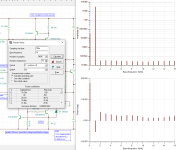
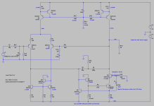
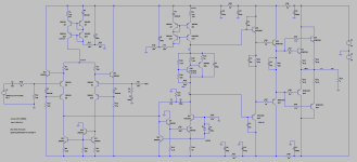
I have created simulation where I isolated IPS and VAS. It is in LTSpice this time - I can see power dissipation if I hover over the element in LTSpice. Neat feature!
There are two versions - one is cascoded and another is not.
Power supply is 44V.
I ramped up current for LTP and VAS to max just to see max dissipation for components.
It is fun
Biasing was shamelessly stolen from the Wolverine schematics lol. I am not sure 100% how it works though. In particular, why do we need additional npn transistor to bias two common base cascode transistors.
The point is that dissipation is 40mW per transistor in non-cascoded LTP and it is down to 20mW in cascoded LTP. Am I missing something?
Attachments
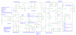
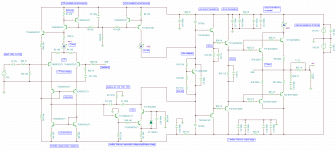
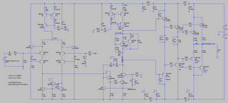
Had some fun working more on this project.
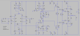
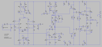
Input stage is cascoded long tail pair now.
BC857C SMD transistors are dual / on the same die and should be matched pretty evenly. Also, min hfe for those is 420.
Buffer transistor is used to bias common base transistors for the cascode. Simple resistor voltage divider. Zener can also be used.
Feedback resistors had to be reduced to 10k and 1k giving 100 SNR.
Simple current mirror without helper transistor.
Question:
what LTP current to use? 5mA like in Wolverine? or 1mA?
Emitter follower VAS using Hawksford enhanced cascode.
Question:
what VAS current is optimal? 4mA?
Simple Vbe multiplier with transistor mounted on the heatsink.
Question:
Should I use dual transistor Vbe?
3EF output stage with base stopper resistors for driver and output transistors. Pre driver transistors are crippled a little with 22p caps.
10mA current for predrivers
20mA current for drivers
Two paralleled output transistors help with low impedance loads as they share the output current equally.
Power rails are progressively decoupled:
first output transistors decoupled with pre-driver and driver,
then, input stage is decoupled further.
Comparing to Wolverine, this design is:
missing ripple eaters (cap multipliers),
missing current mirror helper transistor,
missing Vbe multiplier second transistor.
uses less output paralleled transistors.
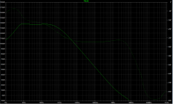
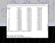
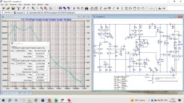
In simulation is able to get 0.0004% THD at 1khz.
With open loop gain of 61dB at 20kHz.
Input stage is cascoded long tail pair now.
BC857C SMD transistors are dual / on the same die and should be matched pretty evenly. Also, min hfe for those is 420.
Buffer transistor is used to bias common base transistors for the cascode. Simple resistor voltage divider. Zener can also be used.
Feedback resistors had to be reduced to 10k and 1k giving 100 SNR.
Simple current mirror without helper transistor.
Question:
what LTP current to use? 5mA like in Wolverine? or 1mA?
Emitter follower VAS using Hawksford enhanced cascode.
Question:
what VAS current is optimal? 4mA?
Simple Vbe multiplier with transistor mounted on the heatsink.
Question:
Should I use dual transistor Vbe?
3EF output stage with base stopper resistors for driver and output transistors. Pre driver transistors are crippled a little with 22p caps.
10mA current for predrivers
20mA current for drivers
Two paralleled output transistors help with low impedance loads as they share the output current equally.
Power rails are progressively decoupled:
first output transistors decoupled with pre-driver and driver,
then, input stage is decoupled further.
Comparing to Wolverine, this design is:
missing ripple eaters (cap multipliers),
missing current mirror helper transistor,
missing Vbe multiplier second transistor.
uses less output paralleled transistors.
In simulation is able to get 0.0004% THD at 1khz.
With open loop gain of 61dB at 20kHz.
Attachments
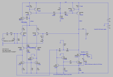
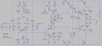
Another iteration, now in LTSpice improves on CCSs for both LTP and VAS. LTP is cascoded and bootstrapped with transistors for each cascoded EF.
Vbe multiplier was upgraded to CFB type.
3EF OPS now has additional parallel pair of output transistors.
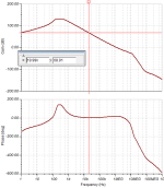
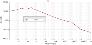
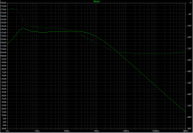
Open loop gain is 80dB at 20kHz.
THD is 0.0002% at 1kHz.
Vbe multiplier was upgraded to CFB type.
3EF OPS now has additional parallel pair of output transistors.
Open loop gain is 80dB at 20kHz.
THD is 0.0002% at 1kHz.
Attachments
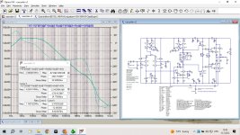
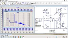
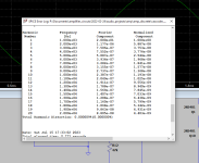
I simulated this .asc file and somothing is very wrong with this amp. First, the output bias is set to more of the 1A (class A?), and LG at 20kHz is about 40dB, PM and GM practically don't exist, look at attached simulation. Could you attach you last .asc file?Another iteration, now in LTSpice improves on CCSs for both LTP and VAS. LTP is cascoded and bootstrapped with transistors for each cascoded EF.
Vbe multiplier was upgraded to CFB type.
3EF OPS now has additional parallel pair of output transistors.
Open loop gain is 80dB at 20kHz.
THD is 0.0002% at 1kHz.
Attachments
Looking nice! You are way ahead of me obviously in the amp design and simulator.Some simplification
But the idea behind using two transistors were to bootstrap each cascode independently.
It can also be biased by just using zeners or LEDs.
I tested for clipping and it looks like adding booster cap around 150p to the BC junction of the CCS transistor helps to reduce oscillations.
Increasing cap to 470p completely gets rid of oscillations while clipping, but increases 20khz THD.
I replaced CCS transistor with another diode as it is more practical to use higher power dissipation transistor instead of dual SMD package like I planned before.
Your OPL looks really nice and flat! I wonder how did you get it?
Thank you for input!
Last edited:
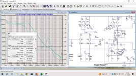
It was working draft and so bias was not set correctly. Also many other minor things were fixed and polished since. I am learning as I go.the output bias is set to more of the 1A
With that said, the latest THD results are much better now.
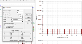
0.000009% at 1kHz
0.000187% at 20kHz
Attachments
Last edited:
Have you looked at Q2 and Q1 Vce? Looks to me like it is pretty much zero - Q13 Vbe +D4 = Q9 Vbe+Q2 Vbe. Same goes for the loop around Q1. If you are keen to cascode each circuit, why doesn’t Q12 have a cascode too?
Check what Vcesat is for Q1 and Q2, as they probably aren’t working as well as you are hoping. In reality, Q9 and Q10 are probably working as the differential pair, rather than Q1 and Q2.
Check what Vcesat is for Q1 and Q2, as they probably aren’t working as well as you are hoping. In reality, Q9 and Q10 are probably working as the differential pair, rather than Q1 and Q2.
At E of Q1 probing voltage gives 816.92mV and at the C of same Q1 215.96mV totaling in 600.96mV. Which is one Vbe drop. Q1 and Q2 therefore need to be low Vce(sat) type.Have you looked at Q2 and Q1 Vce?
Looking up Vce(sat) for 2N5401 datasheet specifies -0.5V
So we are right on the edge.
Diodes can be replaced with green or red LED or 2V zener to allow for wider variety of transistor choices for Q1 and Q2.
I don't see the point as current mirror already performing very good.If you are keen to cascode each circuit, why doesn’t Q12 have a cascode too?
I tried.
All other combinations of CM just don't show as great of results.
Verified by checking currents over R4 and R5.
Hi Guy's,It was working draft and so bias was not set correctly. Also many other minor things were fixed and polished since. I am learning as I go.
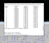
With that said, the latest THD results are much better now.
0.000009% at 1kHz
0.000187% at 220kHz
Just so you have a baseline,
These are the Wolverine's sim numbers at 80w output into 8 ohms
0.000001% at 1k
0.000067% at 20k
We also include trace inductance and capacitance in our simulation if you don't your risk high frequency oscillation.
If you want to reduce the distortion you need to try and modify your topology a little to get more loop gain. The more loopgain you have the more negative feedback you'll have to reduce distortion.
If you're not already I suggest extensive phase and gain margin testing. Follow the loop gain 2 example in ltspice to know how.
For your drivers Q20 and Q25
You may want to see the loopgain improvement using something similar to the Wolverine in that location.
Capacitors on the base rather that to the collector. But extensive simulation is required to get the ideal values
Good luck with your simulations
- Home
- Amplifiers
- Solid State
- Reference discrete amplifier inspired by Wolverine and Cordell book