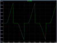
I soldered small film caps between each bridge rectifier legs and before plugging in to full mains I tried with DBT. Well, bulb stays bright and each transformer secondary is 7V AC instead of 18V AC. Is it because of the bypass caps between rectifier legs? I checked my work, there is no short between legs. If I remove these small bypass caps DBT stays dim..
Did I done something wrong?
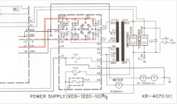
I followed this schematic;
Did I done something wrong?
I followed this schematic;
An externally hosted image should be here but it was not working when we last tested it.
I see no valid reason for the behavior you report; it has to be bad or wrong components, unsuspected short or something of the kind.I soldered small film caps between each bridge rectifier legs and before plugging in to full mains I tried with DBT. Well, bulb stays bright and each transformer secondary is 7V AC instead of 18V AC. Is it because of the bypass caps between rectifier legs? I checked my work, there is no short between legs. If I remove these small bypass caps DBT stays dim..
Did I done something wrong?
I followed this schematic;
An externally hosted image should be here but it was not working when we last tested it.
Anyway, the preferred implementation of what you want to do is with small ceramic disc caps (1 to 10nF, 500V), preferably soldered directly on each diode for good VHF suppression.
Film caps are not as effective
Is the circuit just as shown or have you still got it coupled to and feeding whatever it supplies ?
Edit... sorry, hadn't noticed the bit "If I remove these small bypass caps DBT stays dim.."
Ignore 🙂
Edit... sorry, hadn't noticed the bit "If I remove these small bypass caps DBT stays dim.."
Ignore 🙂
Those capacitors are not snubbers.
All they do is add capacitor and diode capacitance togther, to end up lowering the resonant frequency. Often resulting in worse ringing.
You need a resistor to damp the ringing. It's the resistor that acts as the snubber.
All they do is add capacitor and diode capacitance togther, to end up lowering the resonant frequency. Often resulting in worse ringing.
You need a resistor to damp the ringing. It's the resistor that acts as the snubber.
You have been brainwashed by the "snubbering brigade": try to feed an ordinary AM/FM radio with the the "crude" capacitor version and then the nice, cleanly snubbered one (as seen on an oscilloscope screen).Those capacitors are not snubbers.
All they do is add capacitor and diode capacitance togther, to end up lowering the resonant frequency. Often resulting in worse ringing.
You need a resistor to damp the ringing. It's the resistor that acts as the snubber.
You will understand why asian makers of cheap sets got it right as early as the sixties.
Note that you can do both if you find it comforting, but only one is actually necessary
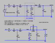
I'm sorry but I forgot to mention something.. And I think this is the root of the symptoms that I have.
This is F5.. with two secondary,two bridge rectifier and fully biased (1.3A per channel) amp. And I soldered caps to bridge as it is and tested with dbt with 25W bulb. And it stayed bright. And I think this is because of amp was fully biased already.. I removed the caps from the bridge, while I'm in there I zeroed offset and bias to readjust. Tried with dbt again and it goes dim all the way... with zero bias...
This is F5.. with two secondary,two bridge rectifier and fully biased (1.3A per channel) amp. And I soldered caps to bridge as it is and tested with dbt with 25W bulb. And it stayed bright. And I think this is because of amp was fully biased already.. I removed the caps from the bridge, while I'm in there I zeroed offset and bias to readjust. Tried with dbt again and it goes dim all the way... with zero bias...
I recommend a multi-band shortwave receiver instead. The ringing can occur at whatever frequency the L's and C's dictate; there is no a priori reason to be confident that this ringing must fall within the AM band or the FM band.try to feed an ordinary AM/FM radio with the the "crude" capacitor version and then the nice, cleanly snubbered one (as seen on an oscilloscope screen).
Changing the value of L and/or C will change the frequency of ringing, which can move it into the AM band or the FM band, leading to the incorrect conclusion that the modification made the situation worse. It is also possible that changing L and/or C changes the frequency of ringing, moving it out of the AM band or the FM band, leading to the incorrect conclusion that the modification made the situation better.
In my own experiments, I've seen transformer leakage inductance L as low as 10uH and as high as 100mH, a range of ten thousand to one. I've also seen secondary resonant capacitance C (= trafo Cmutual + Crectifiers) without any "protection" capacitors added, as low as 60pF and as high as 10nF, a range of 160 to one. So the secondary's natural frequency of oscillation omega_naught, varies by more than a hundred to one; sometimes it falls in the AM or FM band, other times it does not. The claim that an AM/FM receiver is absolutely the best analysis and measurement tool for every transformer+rectifier combination, is not supported by experimental data.
Rectifier diodes typically cause three distinct types of disturbances.
First type is caused by the diode switching exciting the resonance of the transformer's leakage inductance with various capacitances, explicit or implicit.
It is the most visually obvious with an oscilloscope, and it is also relatively easy to cure with an appropriate damping network.
Second type is caused by the snap-off effect of the diode, generating a spray of HF and VHF energy at each current zero crossing. Because the HF level is small, and the recurrence is low (compared to the frequencies of the energy), it is completely invisible on an oscilloscope and even on a traditional, swept spectrum-analyzer. However, it causes a characteristic 100Hz (or 120Hz) buzz in receivers. A damping network for type 1 will dissipate some of the RF energy, but since the damping network has a series resistance, it will leave a significant residue.
In addition, the damping network is normally used once, across the transformer, but each diode (and its associated wiring) acts as a RF generator.
Third type is even more evasive: it is caused by the rectifier diodes behaving as PIN diodes. They change the grounding configuration of the antenna 50 or 100 times per second, and they modulate the apparent level of the incoming RF signal at the same rate, also causing a buzz that typically varies with the placement of cables, hand effects, etc.
There again, a damping network intended for type 1 will mitigate the effects, because there will be some equalization in the impedance variations, but some switching effects will remain.
The cure for type 2 and 3 is more or less the same: a small bypass capacitor directly across each diode. This capacitor acts as a short at RF. For type 2, it confines the RF disturbances to a small space. In principle, a capacitor cannot dissipate anything, and it can only reflect incident energy, but in practice with the values and components used, the confined energy is quickly dissipated. Matters can be improved by adding a small dissipating ferrite bead to the diode: it increases the impedance of the generator, and provides an explicit dissipation means.
For type 3, the capacitor acts by shorting completely all modulation effects.
Typically, the capacitor value is 4.7 or 10nF, but the range found goes from ~1 to 100nF.
See below an example of a typical commercial product.
These capacitors are the only mandatory ones. A "proper" damping network is rarely found on commercial products, because it is generally unnecessary on otherwise properly designed equipment.
Things can be different for amateur gear, for which there is also the "before/after" effect: when the cure is so visually effective, it can only be "a good thing".
It can do no harm anyway, and will always improve matters, but by order of importance the capacitor on each diode (very close) comes first, followed by the ferrite bead, and finally for perfectionists, the optimal damping network.
Attachments
So, there's a type of diode-generated RF noise that's too small for oscilloscopes too see, even with AC coupled (high pass filtered) input and scope trace sync'd/triggered to zero crossings? Not only is this noise too small to see on a scope, it's too small to see on a spectrum analyzer? However it's not too small for a high gain radio receiver to detect it?
How well does a typical audio power amplifier (gain = 21X) detect this RF noise? Phono preamplifier (gain = 2000X)?
How well does a typical audio power amplifier (gain = 21X) detect this RF noise? Phono preamplifier (gain = 2000X)?
A small Hitachi battery/mains radio was my first introduction to this problem. On mains, and there was an annoying harsh buzz when used on FM. On AM it was fine. The fix was to add a 0.01uf directly across the tranny secondary as I recall. I was only a youngster back then and I was pleased to have sussed it out. I seem to remember just touching the diode (it was a half wave rectifier) altered the buzz dramatically.
Years later and a colleague told me of similar problems with his Leak tuner and how it needed a snubber on the mains tranny.
Years later and a colleague told me of similar problems with his Leak tuner and how it needed a snubber on the mains tranny.
Yes, although it is probably visible using the latest digital phosphor scopes.So, there's a type of diode-generated RF noise that's too small for oscilloscopes too see, even with AC coupled (high pass filtered) input and scope trace sync'd/triggered to zero crossings? Not only is this noise too small to see on a scope,
We are talking about mV's here, even less.
Anyway, there has to be a noise, from a theoretical POV because there is a waveform discontinuity and diode recovery phenomenons, however stealth they are with modern semi's, and from a practical POV because you can hear it as a buzz on a receiver. A damping network is not sufficient to kill it completely.
This has to be qualified: I said it was mostly invisible on swept SA's, because of the low duty cycle of the effect. Using a synchronized sweep together with a peak detection mode could probably catch it, but modern instruments working in real time would be better suitedit's too small to see on a spectrum analyzer?
It would be completely insensitive to it. Problem is that amplifiers can be connected to tuners for example, and even when they are not directly connected to receiving equipments, they may cause disturbance to other receivers in the vicinityHow well does a typical audio power amplifier (gain = 21X) detect this RF noise?
Even there, I doubt it could directly cause troubles; maybe in a rare extreme case, but unlikely.Phono preamplifier (gain = 2000X)?
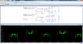
It is probably worth illustrating the phenomenons with a sim.
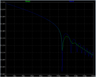
First pic shows a crude, halfwave rectifier completely raw and naked with the transformer's parameters shown explicitly. L1 is the leakage inductance and L2 the wiring to the rectifier.
The parameters of the components are half-realistic; I include the asc, so that they can be viewed or modified.
I show the spectrum at the input of the rectifier, V(a), and also the "clean" V1, because the sim's FFT has more or less the same type of problem as a real world spectrum-analyzer: the parameters are unfavorable, and this raises the noise floor significantly.
At 100Mhz, the floor sits at -185dB and V(a) at -100dB.
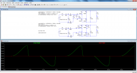
Then, the snubber network is added; values may not be optimal, but adjusting them would change the numerical results by a few dB, and not change the conclusion.
The 100MHz is down a little, but not very much: problem comes from R3: it is basically the circuit of a step-diode frequency multiplier.
Then, the snubber is replaced by a parallel cap. Now the 100MHz level is down by 60dB: a real improvement.
These results are corroborated in reality, which is why all receivers and many other electronic gears have the sempiternel quadruplet of 10 or 4.7nF ceramic caps across the rectifier diodes. Some may have in addition a "proper" snubber, but in reality that's quite rare.
Attachments

Thanks Elvee!
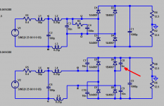
I drew a snubber-across-transformer circuit design on the same .asc simulation page as your capacitor-across-diode circuit, please see schematic below. Then I ran them both in the same LTSPICE run. My simulation .asc file is attached.
I applied a Quasimodo style CRC snubber using the Quasimodo design note's recommended values Cx=0.01uF and Cs=0.15uF.
Since I have already got a "1N4007" in my component lib, I renamed your diode model to "LV4007" just to be certain that I'm using your parameters and not accidentally the ones in my library.
As you can see in the attached transient output waveforms, the CRC snubber is even better than the capacitor-across-diode in removing ring-a-ding-ding wiggles, at least in this one test applied by the simulation jig you kindly provided. Those people "brainwashed by the snubbering brigade" (see post#5) get superior performance in this one test.
Best regards,
Mark Johnson
_
Attachments
In this case, it looks better at first sight, mainly because of Cx, which in the sim plays practically the role of the capacitor across the diode, and because of the additional damping provided by the 50 ohm (BTW, if you increase the capacitors by a factor 10, and reduce the resistor in the same proportion, things will be 10 times better -in principle-).
Things are not that simple however: first, in the case of a full wave rectifier the snubber will be in parallel with two diodes in series, not one, which in sim is not going to degrade things, because everything is perfectly balanced, and anyway disturbances will appear as common mode between the AC and DC sides, but in reality, wiring capacitances and inductances are going to upset the balance, resulting in common mode perturbations.
Another thing to consider if a single network is used is all the inductances of the wires, the filter cap, etc. At VHF, if the loop areas exceed 1 cm², they will begin to act as radiators, and achieving such compactness with a single network is going to be difficult, except perhaps for small SMD circuits.
This is why an individual bypass of each diode remains essential.
That said, these capacitors can become the Cx of your snubber.
There is also the other reason for an individual bypass: to kill modulation effects caused by the PIN behavior of the rectifier diodes. Slow diodes like the 1N4007 work very well in this role, and have even been used as cheap substitute in low-cost antenna switches.
Practically all of the industry has been using the 4-caps only method for decades, at least for 50/60Hz applications (things are different for SMPS's) and probably for a good reason: if the ringing is pushed below the LW band, additional improvements brought by a complete snubber are negligible, while the opposite isn't true: dispensing with individual bypass is always going to cause buzzing in some circumstances.
That said, a snubber has a negligible cost, and does make things nicer, so why not.
But if a proper snubber brings a measurable improvement to an equipment, the first thing to ask is why, because sensitivity to this kind of perturbation equates to a weakness somewhere, and other types of noise could follow the same path...
Perhaps you might be able to build a simulation with four diodes instead of one, which shows these effects more convincingly than hand-waving arguments about what might possibly happen. After all you were able to build a simulation with one diode that showed your cap||diode performed better than (470R series 10n) across the secondary. However CRC was better still.
If imbalance is required in order to see the effect, you could implement it by simulating using four different diode types (e.g. 1N4007, 1N5404, GBPC3510, 6A4) and different parasitic inductance, resistance, and capacitance in the wires. Or just make 4 variations on the 1N4007 with model parameters changed by amounts you deem reasonable. If the effect is real then shouldn't you be able to simulate it in SPICE?
If imbalance is required in order to see the effect, you could implement it by simulating using four different diode types (e.g. 1N4007, 1N5404, GBPC3510, 6A4) and different parasitic inductance, resistance, and capacitance in the wires. Or just make 4 variations on the 1N4007 with model parameters changed by amounts you deem reasonable. If the effect is real then shouldn't you be able to simulate it in SPICE?
The lumped representation of leakage inductance and shunt capacitance perhaps should also have a lumped ESR. Any main filter cap ESR is probably inconsequential.
A transmission line model of the secondary winding may be of more insight.
A transmission line model of the secondary winding may be of more insight.
It should be possible:If imbalance is required in order to see the effect, you could implement it by simulating using four different diode types (e.g. 1N4007, 1N5404, GBPC3510, 6A4) and different parasitic inductance, resistance, and capacitance in the wires. Or just make 4 variations on the 1N4007 with model parameters changed by amounts you deem reasonable. If the effect is real then shouldn't you be able to simulate it in SPICE?
The test setup is now upgraded to full wave, and adapted to a proper measurement of common-mode effects.
On the DC side, this simply means splitting the load in two, and connecting GND at the junction (C1 could also be split, or it could be done with waveform math).
On the AC side, the circuit has been symmetrized, and the common-mode is extracted by displaying the arithmetic average of the voltages at the transformer's terminals.
Diode 1A4007 is the untouched 1N4007 model and 1B4007 has a single parameter changed: the capacitance Cjo is now 20pF instead of 28pF.
First pic shows a dry run, to make sure the setup has no flaw. The common-mode is indeed zero, or practically:
The snubbered one shows a very tiny voltage, which already indicates a greater susceptibility: in order to ease the convergence, LTspice slightly degrades the ideal perfection of the pure sim, which causes higher order effects to be marginally visible.
Second pic shows the situation with one of the 4 diodes replaced by the deviant one.
For the unsnubbered version (red), there is practically no change, but the snubbered version leaks a considerable amount of common-mode perturbation, because the unbalance is raw, not mitigated by the much larger 10nF's.
This common-mode appears between the equipment ground and the transformer's secondary, which itself is coupled to the primary and therefore the mains via the interwinding capacitance, and from an average AC point of view, the mains is equivalent to the ambient space and the earth.
This kind of common-mode interference issue is the most problematic (compared to differential ones), and is the target of the majority of the suppression components: mains filters, common-mode chokes, "Y" capacitors.
However, eliminating the problem at the source is always a better option than stacking CMC's a posteriori.
In practice, even with bypass caps, some leaks may remain because there are many other mechanisms involved, and it is preferable to use CMC's as a last resort, to perfect the job if it is still required
Attachments
Hi Elvee
Excuse me for my ignorance. CMC as in common mode chokes ? If it is for a power
amp are these available for high current applications & do we place it after the rectifiers
or ?
Thks
Excuse me for my ignorance. CMC as in common mode chokes ? If it is for a power
amp are these available for high current applications & do we place it after the rectifiers
or ?
Thks
Thanks Elvee!
I ran your LTSPICE simulation circuit file (.asc) in post #17. I discovered that the bottom circuit is very sensitive to mismatch between the capacitors-across-diodes. Figure 1 shows the schematic with three perfect 10.00 nanofarad capacitors and the fourth capacitor 10% low. The common mode voltage at (G+H)/2 is big.
So, if you are at all worried about common mode voltage, and if you intend to apply capacitors across rectifier diodes to eliminate it, then please select four capacitors that are all within 1% of each other. 0.5% would be better still. I'm confident that makers of table radios with inbuilt linear power supplies, use super-tightly-matched capacitors in these positions.
By the way, 0.25uH for L4 and L5 corresponds to about 20cm (eight inches) of AWG20 wire. Rather a pessimistic overestimate of the distance between the transformer and the rectifiers.
_
Attachments
Hi Elvee
Excuse me for my ignorance. CMC as in common mode chokes ?
Yes
They exist in a large variety of values and current ratingsIf it is for a power
amp are these available for high current applications &
Basically, you don't need one, and you shouldn't use one for decorative purposes, just in case, at least for a 50/60Hz supplydo we place it after the rectifiers
or ?
.
Yes, that is in substance what I said earlier: the configuration, with or without caps relies on balance to eliminate the common mode. After all, a bridge rectifier is a bridgeI ran your LTSPICE simulation circuit file (.asc) in post #17. I discovered that the bottom circuit is very sensitive to mismatch between the capacitors-across-diodes. Figure 1 shows the schematic with three perfect 10.00 nanofarad capacitors and the fourth capacitor 10% low. The common mode voltage at (G+H)/2 is big.
In fact, these capacitors are always of the cheapest variety, ceramic disc or MLCC, and they certainly have significant mismatches causing the apparition of a significant common mode voltage, but this does not really matter, provided they are large enough.So, if you are at all worried about common mode voltage, and if you intend to apply capacitors across rectifier diodes to eliminate it, then please select four capacitors that are all within 1% of each other. 0.5% would be better still. I'm confident that makers of table radios with inbuilt linear power supplies, use super-tightly-matched capacitors in these positions.
To understand why, it is preferable to adopt a more general approach. The conclusions will be applicable to many other sub-cases.
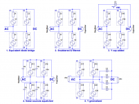
Each diode can be seen (and actually is) a noise source. From this point of view, the bridge rectifier circuit can be replaced by 4 noise sources having a certain internal impedance, see (1.)
It is clear that such an arrangement will generate differential noise on both the AC and DC ports, and common mode noise between the two.
Now, you connect your perfect snubber to the AC side, and your ideal filter cap to the DC side. Since both are perfect shorts, the circuit becomes 2: you have eliminated all the differential perturbations.
The common mode perturbations will remain though. Problem, you have used all your shots: if you don't want to add something else, be it a capacitor or a snubber, the only way that the CM could be zero is if the 4 noise sources follow precise correlation rules: with 4 independent sources, you have 4 degrees of freedom, and that's 4 too many.
Under ideal sim conditions, the correlation criterion will be met: all the diodes are identical, there is no external parasitic effect or element, and they receive exactly the same stimulus and they thus give exactly the same response.
In reality, things will be different: even if you were crazy enough to try to match the diodes (which would be very difficult, because all the parameters need to be accurately matched), you would still have the problem of matching the layout and wiring to a VHF grade, which is not simple.
If you want to eliminate or at least reduce the common-mode noise without matching, you have some options:
The first and most obvious is to select lower noise sources, ie better diodes. Let us rule that out because of cost, and because there is a theoretical floor to that approach. Even with no recovery artifacts, a diode remains a switching device, creating discontinuities and therefore harmonics.
Another possibility is to make the AC and DC sides equipotential at the frequencies of interest. To do that, you need to connect a sufficiently large cap between the AC and DC sides, a Y cap (3.)
Since both the snubber and the filter cap are perfect, you can choose indifferently any of the terminals.
Here, for low voltage applications the Y cap only plays that role, but it doesn't need to be a true safety cap.
In reality, this Y cap would be connected to the mains side, because the ultimate goal is to make the user ground equipotential with the mains = ambient space: the secondary winding is just an intermediate step, and it is preferable to bypass it directly.
Yet another option is to reduce the noise to insignificant levels at the sources themselves: this will reduce all categories of noise, and also make the system more tolerant to imbalances in the same proportion.
This can be done by shorting the sources with suitable capacitors (4.)
According to your doctrine, not all 4 Cb's are required: since both the AC and DC ports are perfect shorts, only one capacitor would in fact be necessary, and the circuit could be degenerated to (3.)
As you noted, mismatches in the Cb values will generate common mode voltages, but at lower frequencies mainly, because for RF the Cb's have already played their attenuating role.
The most extreme case of mismatch would be for the single Cb case.
These solutions are suited to the perfect snubber/perfect filter cap situation, but they need to be adapted for a more general approach: with no or an imperfect snubber and a filter cap that doesn't remain a perfect short at high frequencies, simplifications are no more possible: for the case (4.), this means using all 4 caps, and for the (3.), some additional components will be required:
To make sure the AC and DC sides are fully equipotential, and to eliminate mode conversion mechanisms, each AC terminal needs to be connected to each DC terminal, that is a total of 4 capacitors (5.)
But in reality, the cap configuration is the same as (4.).
This means that the capacitors can be merged, and only 4 are required in total to implement both techniques of CM noise reduction.
The capacitors will also contribute to the reduction of the differential noise, and eliminate the PIN modulation effect.
That is a lot of birds killed with single stone, and that is the reason why it is almost universally adopted.
Note that all of the above only makes sense from an electromagnetic compatibility perspective: an amateur just interested in audio doesn't have to worry about it, because it will normally have no detectable impact.
Attachments
- Status
- Not open for further replies.
- Home
- Amplifiers
- Power Supplies
- Rectifier Diode Snubber;