I use KiCad and am reasonably happy with it. I like the fact that it has no limits on board size, and it has no limits on layer count, and that it's completely free and open source. Last time I checked, many of the other alternative PCB layout programs charged extra for "advanced features" like large boards and >2 layers.
EasyEDA: either online of offline where you can syn. Easy drag and drop
Select "User Contributed" part list as much as you can since it will be a correct size
Some of the tube lists don't have filament so if you plan to have filament on the PCB, then pick the right one otherwise, it will be crazy to fix later to change the part. It's best to pick the one with filament even you don't make connection.
KiCad is very capable and free.
I've used this for PCB including adding my own footprints but adding your own 3D models requires some additional CAD software to make the component 3D model etc. There are valve foot prints for sockets etc. There's also a number of great directory resource sites for library components too.
The annoying thing is it doesn't import LTSpice.. but can run it's own spice sims based on the schematic that's been drawn.
Our friend Nigel https://www.diyaudio.com/forums/members/nigelwright7557.html who regularly posts in this Forum makes an EXCELLENT PCB design software.
Murton-Pike Systems PCBCAD51 pcb design software - Murton-Pike Systems PCBCAD51 PCBCAD PCB CAD printed circuit design software.
Not "free" as in it costs all of FIVE Pounds , practically Mailing price, with the great advantage that Designer is available right here so you can ask anything one-on-one.
That alone is worth a lot.
I will second EasyEDA - Online PCB design & circuit simulator
The fact it runs in a browser well means that it works for people like me who don't use Windows (Linux all the way).
Maybe Merlin can tell us if his PCBCAD will run under WINE.
The fact it runs in a browser well means that it works for people like me who don't use Windows (Linux all the way).
Maybe Merlin can tell us if his PCBCAD will run under WINE.
Last edited:
I use DesignSpark PCB also free. It's definitely not perfect, I don't think any of these are. I started to learn Eagle but the board size limitations did not work for vacuum tube work.
Whatever you use I'd pick one and stay with it as they seem different enough to be irritating to switch.
Whatever you use I'd pick one and stay with it as they seem different enough to be irritating to switch.
Welcome to PCB Elegance! | PCB Elegance
It was a commercial product, now open source. Schematic capture and pcb design.
It was a commercial product, now open source. Schematic capture and pcb design.
KiCad runs on Linux and the library is impressive, even for 3D models.
same here. I downloaded many 3-D models for free from https://www.3dcontentcentral.de/. Before downloading you can choose the desired format. Alternatively freecad (on lInux) can do format conversions for you.
Over 1 million models in EasyEDA. I've never had to create a model/footprint. Find a part on LCSC that fits, and use it's outline  There's no model for 6F12P (that I know of) so I use 12AX7. I design the board without making a schematic either - just "connect the dots". I use SchemeIt on DigiKey for schematics.
I use DipTrace and find it very good.
DipTrace - Schematic and PCB Design Software
DipTrace - Schematic and PCB Design Software
I think autodesk made eagle freeware again./QUOTE]
I started with Eagle 2.6 for DOS in 1992. I paid for nearly every upgrade until Windows version 5.11 when Newark / Farnell bought them and raised the price. Then Autodesk bought it and asked $600 per year for a subscription that would allow 50 square inch boards and commercial use. Agreeing to this lease required forfeiting your previous license, so they would kill my V5.11 making it impossible to go back.
Tubelab doesn't make enough profit in most years to afford that, and Autodesk's restrictive agreement is a deal breaker, so I'm still using V 5.11.
To make things even harder the library formats have changed at least twice since V5.11. The new versions can read the old libraries, but my old V5.11 can not read any library from V6 or later.
Autodesk does have a free download which is limited to two schematic sheets, single side or two sided boards (no 4 layer boards) and 80cm2 (12.4 sq inches) maximum board size. No commercial use is allowed.
The free version I downloaded about 2 years ago did "call home" to Autodesk for authorization on start up. It would not open if the Ethernet cable was pulled from the PC. It is not clear if using the free version to open a schematic I downloaded from the web could jeopardize the Eagle V5.11 that I have paid for, so I have removed it from my PC.
I have downloaded and installed KiCad, but have not taken the time to really learn it. I used Cadence and Mentor Graphics PCB layout software at work. As with all of these layout packages, learning the basics takes time, practice, and the creation of a big "cheat sheet."
Eagle had its quirks, but I worked at an off campus think tank in the early 90's which was about a mile from the Cadsoft US office, so their tech guy knew me well. After a year or so I could make Eagle do things he couldn't imagine.
Learning how to trick Mentor into doing what I wanted, not what the Motorola corporate design rules forced, took several years. Then they switched us all to Cadence. Note that I did not design boards for Motorola products. I designed prototypes and test fixtures. For those, the only rule is "does it work?"
Not that I have ever done this, but it is possible to make several small boards in a size restricted design package and stitch them together in a drawing program if you DIY your own boards. I believe that you could use a Gerber editor to splice together small Gerber files, but it might not be worth the work or risk of screw ups.
Tube Circuits don't have nearly as many nodes and connections as a computers motherboard. So I never saw a need for autorouting, and I enjoy the process of "just drawing it". I use Sprint Layout. I'm very much a tube Newby but here are a few examples of stuff I drew: I've binged out and ordered about 25 different board designs since August, its fun.
Sprint Layout 6.0, ELECTRONIC-SOFTWARE-SHOP
Elliott Sound Products Capacitor multiplier top and bottom
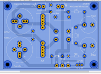
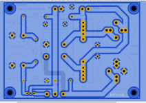
Salas 6V6 mono on tiny board, the cathode circuit goes on a plug edge card so I can experiment so no K circuit parts on the board just an edge card socket)
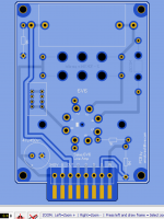
A Novar breadboarding jig (this one has a few mistakes but it works, the center hole is off). This uses 5.08 pitch spring clips for the hookup.
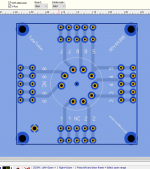
A general purpose bridge rectifier with Quasimodo snubber, fused secondary, bleeder, first reservoir, and lamp. Sometimes I do ground plane to ground plane jumpers when I see that I've split the ground plane with a long trace. This one uses 4 layers so I could have a full power plane and ground plane under the reservoir cap, big charging pulses. It can use a variety of capacitor sizes or counts.
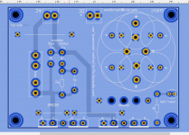
Sprint Layout 6.0, ELECTRONIC-SOFTWARE-SHOP
Elliott Sound Products Capacitor multiplier top and bottom


Salas 6V6 mono on tiny board, the cathode circuit goes on a plug edge card so I can experiment so no K circuit parts on the board just an edge card socket)

A Novar breadboarding jig (this one has a few mistakes but it works, the center hole is off). This uses 5.08 pitch spring clips for the hookup.

A general purpose bridge rectifier with Quasimodo snubber, fused secondary, bleeder, first reservoir, and lamp. Sometimes I do ground plane to ground plane jumpers when I see that I've split the ground plane with a long trace. This one uses 4 layers so I could have a full power plane and ground plane under the reservoir cap, big charging pulses. It can use a variety of capacitor sizes or counts.

Last edited:
Learning how to trick Mentor into doing what I wanted, not what the Motorola corporate design rules forced, took several years. Then they switched us all to Cadence. Note that I did not design boards for Motorola products. I designed prototypes and test fixtures. For those, the only rule is "does it work?"
Could be worse you know… you could just as easily been working somewhere where product designers have to design/develop all their own eval boards, and said boards have to follow all the corporate design rules and procedures *including the entire supply chain for components*, and assembly must follow a production flow. That’s right - not being able to buy @#$&*% bypass capacitors from Mouser.
For my own projects, I’ve been using an ancient PCB design program I picked up for something like $60 15 years or so ago. It’s called Rimu PCB - still running on an old XT desktop. No idea if it’s still around in some form. I have run into the node limitation in the schematic capture (I didn’t buy the expensive option) but I almost always just draw the board. Put the big fixed location parts down (connectors, filter caps, power transistors) then fill in everything around them. The board will go as big as you like - 17 inches on a side is as big as I’ve ever had to do. I can put big schematics on multiple pages when I hit the 500 net limit.
In the past I've used Protel and OrCAD as well as Cadence's schematic and layout tools for IC design.
I recently started exploring KiCAD. It's definitely capable.
The most recent version is 5.1. I'm not a fan of the schematic editor in that version. It's very "1990s Solaris" in its paradigm. Click to select a component? No. That's not supported. Click-and-drag? Nope! No, you have to hover over the component and then hit a hotkey. Lame! But it does work.
KiCAD 6 by contrast is a joy to use. Now, KiCAD 6 is not out yet, so when I say "KiCAD 6" please substitute the latest v. 5.99 nightly build. The schematic editor now works like any other CAD program. You can even set the zoom/pan/scroll options to a "mouse default" or a "touchpad default", which makes it possible to use touchpad gestures for navigation. It's pretty sweet. I love the spreadsheet tool for editing the properties on multiple components at the same time.
KiCAD 6 supports copy-n-paste between two different schematics, which I don't think 5.1 does.
Symbol and footprint creation is pretty fast and there are scripts to get you going with many standard configurations.
The layout tool is definitely the strong point of KiCAD. It's very capable and as with any tool it takes a bit to learn the various features. I do like the dimming feature (i.e. the trace I'm routing is shown brightly where all other traces are darker). KiCAD 6 supports curved lines in the rats nest, which makes it easier to group components. You can click a button and have regular straight lines for component alignment and such. It also support routing of differential traces, length-matching of traces, etc. It's pretty sweet. And it spits out Gerber files so you can take the files anywhere for manufacturing.
I love that KiCAD is available (even in the nightly builds!) for MacOS and various linux distributions. And Windoze too, naturally. I really appreciate the pricing. It's free (open source), but they accept donations. I'll start donating to them once I start seeing revenue from the projects I've designed with it.
I highly recommend it.
One thing to keep in mind regardless of which software you choose is that you will always find some component that isn't in the software. That's just a fact of life. So I wouldn't make "must have a tube library" a selection criterion. It'd take you an hour or two to define the tube symbols you need.
I'd choose software that does not have any significant limitations on the number of nodes, board size, number of layers, etc. and that outputs Gerber files.
Tom
I think you mean XP .For my own projects, I’ve been using an ancient PCB design program I picked up for something like $60 15 years or so ago. It’s called Rimu PCB - still running on an old XT desktop.
Although some of the **early** DOS programs could run on an XT with EGA graphics.
I´ve been using DOS Protel Autotrax since ´'92 or so and still keep a dedicated XP machin for it (and others) since I have hundreds of designs made with it which still sell like hot cakes , along the years have built up huge libraries for Argentine made pots, switches, jacks, connectors, etc. so woud have to recreate all of them for new soft.
Believe it or not, I am NOW running it in a DOSBOX window, in this very notebook (Windows 7) , designing a small hybrid Guitar amp, some 35-40W, with a 6N2P in the preamp for tube flavour and distortion and a couple TIP121/126 in the power amp, fed from a Conventional EI iron transformer.
Old school solid design, on an old school solid package, match hand in glove
Aiming squarely at same market as Orange Microterror or Joyo Bantam, which are big sellers around here.
So those old workhorses still can provide very decent results.
Didn´t get into modern feature full programs for various reasons: Free versions are size limited while my guitar preamps can be up to 60 cm long (full combo panel width carrying all pots, jacks, switches, even the Power Led), they include tons of features I will never ever use, Libraries with 100000 components drive me crazy, etc. , WHO needs all that Digital crap, microprocessors, memories, AD-DA converters, etc?
Many will, definitely not me
That Protel Autotrax 1.61 is free, has no size limitations (I guess 4 ft by 4 ft) , 8 layers which I will never use, no pin limitations, etc. , is just the icing on the cake.
Guess old style gerbers created by it are not currently recognizable, no big deal for me who will always home make PCBs.
- Home
- Amplifiers
- Tubes / Valves
- Recommended PCB software