Hi all. I am populating a PCB today and ran into a problem. I have to mount 4 on these on this PCB but don't know how to read the symbol to ensure the right direction. I've spent an hour looking on Google with no luck. It is 101 degrees out and I'm working in the garage so I don't mind the break.
Attachments
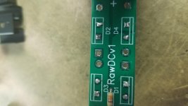
Cathode is on the left. It's always best to verify with your meter before soldering, though.
Also, the close double lines indicate the (insulated) tab side of the package.
The square pcb pad indicates (left) pin #1, which in this case is the cathode.
https://www.mouser.com/datasheet/2/389/cd00000819-1795503.pdf
Also, the close double lines indicate the (insulated) tab side of the package.
The square pcb pad indicates (left) pin #1, which in this case is the cathode.
https://www.mouser.com/datasheet/2/389/cd00000819-1795503.pdf
Last edited:
For current parts, you can just google the part number, and a data sheet will be near
the top of the page. The part pinout ID is always in the data sheet. The variety of package
is typically indicated by the last characters (usually letters) of the complete part number.
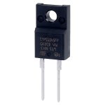
STPS1545D.......TO-220AC.........bare tab
STPS1545FP......TO-220FPAC......insulated tab
STPS1545G.......D2PAK..............smt
the top of the page. The part pinout ID is always in the data sheet. The variety of package
is typically indicated by the last characters (usually letters) of the complete part number.
STPS1545D.......TO-220AC.........bare tab
STPS1545FP......TO-220FPAC......insulated tab
STPS1545G.......D2PAK..............smt
Last edited:
Yep I have the data sheet. I just didn't understand the direction by the double back line. The round diodes have the line at one end of the rectangle that match the silver line on the diode.
The silk-screening is just the part outline as viewed from the top, normally, but here the thickness of an insulated tab causes confusion - the thin rectangle must be the tab, because most TO220 are bare metal tab.
But this is irrelevant as you should check the device and PCB layout to confirm the correct orientation (don't rely on the silk screening being correct).
But this is irrelevant as you should check the device and PCB layout to confirm the correct orientation (don't rely on the silk screening being correct).
- Home
- Amplifiers
- Tubes / Valves
- Quick question about diode symbol on PCB