There are many variations to Diamond buffer. I tried searching Internet and I I am still confused. So I am asking a few questions which might very basic or dumb. I read dugulus self and bob corwell but could not really find the answers to my question.
I would like to know how they differ in operation and why to chose these changes over vanilla version 1.
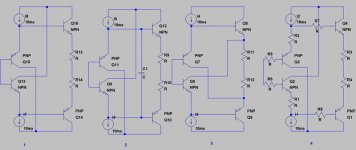
1. addition of base capacitor, what does it do, and how it is calculated.
2. addition of emitter register at input stage, what does it do, and how it is calculated.
3. addition of base register, what does it do, and how it is calculated.
4. In some diamond buffer, driver transistors are connected to power rail but in some variants driver transistor is tied to output transistor instead of power rails, why is that, what benefit does it offer?
5. how to calculate optimum bias current for diamond buffers
http://www.diyaudio.com/forums/attachment.php?attachmentid=645249&stc=1&d=1510466104
I would like to know how they differ in operation and why to chose these changes over vanilla version 1.
1. addition of base capacitor, what does it do, and how it is calculated.
2. addition of emitter register at input stage, what does it do, and how it is calculated.
3. addition of base register, what does it do, and how it is calculated.
4. In some diamond buffer, driver transistors are connected to power rail but in some variants driver transistor is tied to output transistor instead of power rails, why is that, what benefit does it offer?
5. how to calculate optimum bias current for diamond buffers
http://www.diyaudio.com/forums/attachment.php?attachmentid=645249&stc=1&d=1510466104
Attachments
Hi,
1. the cap smoothes and stabilizes the base voltage differential and hence the idle current through the output transistors. Typical values range from 100nF up.
2. Emitter resistors linearize the transistor and ´reduce´ the tolerance sensitivity of the circuit. At the same the voltage drop over the resistors R1/R2 increases the Vbe of the output transistors and hence their idle current. To get back to the same idle current as wo R1 and R2, R3 and R4 need to be incresaed in value also.
3. Base resistors are typically used to reduce the risk of oscillation. Typical values range from 10R to 1k.
4. The collector-emitter connection introduces a kind of feedback that reduces THD (cross-coupling). The input transistors run on a quite constant and very small Vce -almost 0V- which keeps their heat power losses and THD low.
Their idle current of the input transistors is routed through the power transistors though and subtracts from the current through the emitter resistors R3 and R4 and hence from the maximum possible load current. If one increases idle current through the output transistors to counter for that loss the heat power losses of the power transistors will increase.
5. Optimum bias depends on the chosen devices and the attached load. Typical small signal transistors like the BC550/560, BC327/337 behave well around 1-4mA of bias. The bias shold be chosen high enough to supply the output transistors with sufficient base current. Theirs bias current depends on the attached load´s voltage and current requirement.
For line-level voltages feeding into 10-100kOhms 5-15mA are more than sufficient so that the output transistors are working under class-A conditions under all circumstances. If loading is too heavy the diamond automatically slides in class-B, but THD rises considerably (in the amount of harmonics, as well as the amplitude of the harmonics).
jauu
Calvin
Thanks for easy to understand answers Calvin.
So essentially you are saying that Variant 3, with emitter and collector tied together is better.
I read elsewhere that Variant 2, where capacitor has been added, it transformers the circuit into push-pull configuration.
So essentially you are saying that Variant 3, with emitter and collector tied together is better.
I read elsewhere that Variant 2, where capacitor has been added, it transformers the circuit into push-pull configuration.
Did you mean very low Vce or very low Vcb?.......................
4. The collector-emitter connection introduces a kind of feedback that reduces THD (cross-coupling). The input transistors run on a quite constant and very small Vce -almost 0V-
which keeps their heat power losses and THD low.
Their idle current of the input transistors is routed through the power transistors though and subtracts from the current through the emitter resistors R3 and R4 and hence from the maximum possible load current. If one increases idle current through the output transistors to counter for that loss the heat power losses of the power transistors will increase.
.................
Hi,
well, in this case I'd say it hardly matters .... with just a few mV difference between Vce and Vcb.
jauu
Calvin
well, in this case I'd say it hardly matters .... with just a few mV difference between Vce and Vcb.
jauu
Calvin
?
If you have Vbe ~ 600mV and Vce = ~600mV then you will find that Vcb is ~ zero volts.
It makes a lot of difference.
compare to Vce =0mV to 200mV operating conditions.
What will Vbe turn out as?
Will the transistor pass current?
Will a change in voltage at the base control the current passing through the transistor?
Hi,
due to the voltage drop over the output transistor´s emitter resistor, the Vce of the input transistor will always be slightly higher than it´s Vbe, hence >~600mV.
jauu
Calvin
due to the voltage drop over the output transistor´s emitter resistor, the Vce of the input transistor will always be slightly higher than it´s Vbe, hence >~600mV.
jauu
Calvin


Q5 and Q6 are the cascodes.Hi BesPav, may we know how the Q5 Q14 cascode is benefitting us?
I am looking for a diamond OPS for my power amplifier. 200W/8.
Bipolar and also an all MOSFET one. Anything already done by someone?
THx-RNMarsh
Bipolar and also an all MOSFET one. Anything already done by someone?
THx-RNMarsh
Why?? Wanna build in oscillations?
Hi, Calvin!
From the OLG plot i see the unconditionally stable amp.
Hi BesPav, may we know how the Q5 Q14 cascode is benefitting us?
They facilitate mode of operation and in case of power devices helps with Cob effects.
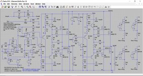
Cascodes could also be supplied from output like this:

I am looking for a diamond OPS for my power amplifier. 200W/8.
Bipolar and also an all MOSFET one. Anything already done by someone?
Not good idea at all.
Too high power, too high bias for input devices due to high base current of latter.
Too high dissipation for one power device, so you need at least three and further increase input current.
It’s better to use EF triple.
They facilitate mode of operation and in case of power devices helps with Cob effects.
Cascodes could also be supplied from output like this:
View attachment 646444
Thanks BesPav for your reply, yes I can understand the power handling, but the circuit as posted earlier doesn't limit the effect of Cob, it only transfer the Cob "problem" from Q5 to Q14 via zener D3, however your new attachment does work as intended to limit the effect of Cob seen by the Q2//CCS node.
@horizonrays
John Broskie @ Tubecad has interesting blog about diamond buffers, worth reading: Might Diamonds
John Broskie @ Tubecad has interesting blog about diamond buffers, worth reading: Might Diamonds

I have been playing with a simulated diamond buffer in various forms for some time. This one uses dual die lateral fet's and being bridged allows a modest single rail to be used for a DC coupled amp. Bias would be switchable. Low impedance load capability is excellent.
Attachments
What about ccs modulated by signal?Not good idea at all.
Too high power, too high bias for input devices due to high base current of latter.
Too high dissipation for one power device, so you need at least three and further increase input current.
What are the tappings A thro' H for?
To allow two different bias settings, 'normal' and 'low' for super cool running.
The fet and its series resistor is placed in parallel with the appropriate resistor on the main circuit when the floating gate voltage is present.
- Status
- Not open for further replies.
- Home
- Amplifiers
- Solid State
- Questions regarding diamond buffers.