I have been using a VI limiter in my amplifier design and it seems to cause more trouble than its worth. The problem is that I haven't found a good alternative that is simple enough to be foolproof to implement.
The problem is, the VI limiter kicks in where there is even a brief spike on the input that drives the input to the rail. The VI limiter transistor, or some other transistor, will usually immediately exceed SOA and be damaged with the result being the fuse is blown on the amplifier. This seems to be because the VAS provides more current than the VI limiter transistor can handle. Limiting the VAS current (even temporarily) seems to have a negative effect on distortion. Ultimately, it seems like the feedback tends to force the current in some part of the amplifier to become high to compensate for the limiting of the output current by the VI limiter.
Other solutions seem less than satisfactory. Speaker fuses can be nonlinear, and speaker relay contacts can be welded shut or become pitted and cause problems. I don't care if the amplifier shuts off, only that it saves the speaker and hopefully itself.
It seems to me that any solution must simultaneously shut down the whole amplifier to prevent the feedback from going to an extreme level in some part of the amplifier. The solution I thought of was to perhaps to put MOSFET switches in the power rails of the amplifier to shut the power down quickly in the even of an output short circuit for example.
I have read about the other solutions in Bob Cordell's amplifier book. For example, flying catch diodes don't seem to kick in except at very high currents, and he also suggests using a TRIAC to shut down the base bias circuit if there is an overcurrent. Has anyone tried these? In simulation, the TRIAC seems to have similar issues where the VAS will deliver too much current to it and could be damaged.
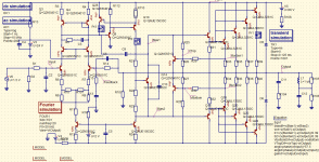
Here's an attachment.
I presently have both a VI limiter and a TRIAC shutdown circuit in there.
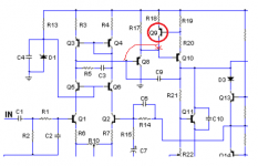
The VAS consists of Q10 and Q12 with Q8 acting as a common collector to not load transistor Q3. One problem is that when Q13 turns on to perform V-I limiting, Q10 supplies more current than it can handle. A current limiter can be placed on Q10, but then Q8 still tries to force Q10 to a particular voltage.
The original AmpsLab c300 the schematic is based on has a Q9 resistor:
https://www.ampslab.com/c300.htm
to limit the current through Q10, but I found it did not work either in simulation or in practice, because when the VI limiter turned on, the Q9 collector pulled too much current as possible from Q8, burning it out.
I have examined many schematics of amplifiers and have not found one where the protection seems to be satisfactory and really protects both the amplifier and the speaker.
I presently have both a VI limiter and a TRIAC shutdown circuit in there.
The VAS consists of Q10 and Q12 with Q8 acting as a common collector to not load transistor Q3. One problem is that when Q13 turns on to perform V-I limiting, Q10 supplies more current than it can handle. A current limiter can be placed on Q10, but then Q8 still tries to force Q10 to a particular voltage.
The original AmpsLab c300 the schematic is based on has a Q9 resistor:
https://www.ampslab.com/c300.htm
to limit the current through Q10, but I found it did not work either in simulation or in practice, because when the VI limiter turned on, the Q9 collector pulled too much current as possible from Q8, burning it out.
I have examined many schematics of amplifiers and have not found one where the protection seems to be satisfactory and really protects both the amplifier and the speaker.
Attachments
Hi profdcd9
I see several things to add, verify or change.
1. Add delay to the VI circuit. Cap across R26 & R27
2. Add base R’s to Q5, Q6 or verify they are stable?
3. Add current limiter to Q10.
Duke
I see several things to add, verify or change.
1. Add delay to the VI circuit. Cap across R26 & R27
2. Add base R’s to Q5, Q6 or verify they are stable?
3. Add current limiter to Q10.
Duke
Topology Tweak
Move the collector of Q9 from its current location to the base of Q8.
You might have to tweak C9 a little...it depends on how big Q9 is.
Check it for stability under limiting behavior.
Move the collector of Q9 from its current location to the base of Q8.
You might have to tweak C9 a little...it depends on how big Q9 is.
Check it for stability under limiting behavior.
48v rails in combination with 4 pairs of output bjt’s.... I would remove the VI limiter. I can make you a quick simulation regarding SOAR Tomorrow if you would like.
You might be able to back off on the protection limits...but you still need something to prevent short circuit disasters.
see enclosed upload
You might be able to back off on the protection limits...but you still need something to prevent short circuit disasters.
I tried what you suggested and it seems to work. I don't know why I didn't think of that before. It seems like the sensible thing to do.
I did a simulation of it with a short circuit. The VAS current is limited to about 25 mA and the output transistors have some spikes of 20 volts (due to inductance). But it seems like this would be much less likely to cause a disaster.
I'll have to give it a try.
Thanks!
Attachments
Yes...I think the driver should be a bunch happier now...
My only concern would be a short circuit on the output of the amp...that was what I had in mind because I hadn't looked carefully enough, and mad a bad assumption!
My only concern would be a short circuit on the output of the amp...that was what I had in mind because I hadn't looked carefully enough, and mad a bad assumption!
Where are the collector diodes on the VI limiter transistors? Normally these are needed to prevent bad-driving the limiters in the opposite cycle at high output levels.
Some thoughts on VI limiters.
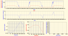
Here’s a pdf of my spreadsheet for a two slope VI limiter, Fig A, whose calculations are derived from Michael Kiwanuka’s* analysis of his Fig 41 arrangement, but with Vref at 0V, a fairly common arrangement e.g. the Leach amp, (but without R1).
Admittedly, a single slope VI limiter is adequate for four MJL3281 devices at 48 volt rails. A two slope might eliminate one device pair, though.
While the location of Q9 collector seems to have solved your issues, I’m puzzled by the limiter plots given by the values of R25 (R28). Ampslab has R25, R28 as 3k3. Your Kicad. sch has a value of 6k8, so has a different slope. (Shown here as R25 3k3 and R25 6k8). Neither appears fully effective, the latter slope violating the SOA curve, while the former intercepts the reactive loads and activates protection much too early.
I’ve used a value of 0.55V throughout as the Q2 (your Q13) trigger Vbe. This Vbe value is crucial to the location of the VI limiter and I don’t claim it to be correct. You have to start somewhere, but 0.6V, usually accepted for these calculations, appears to me, and others, to be too high. Has anyone any example of what it should be? I know, it depends: on the device, the temperature etc. I noticed, though, that if I drop Vbe to 0.4V the R25 6k8 plot is almost identical to my single slope plot. Can your spice schematic verify this?
Can LTspice reproduce some semblance of this spreadsheet? I’m nowhere near familiar enough with it.
Does the above make sense? Any “OMG he’s an idiot” errors?
Thanks for reading.
Brian.
* Found on Bonsai’s web site.
Attachments
- Home
- Amplifiers
- Solid State
- question of VI limiter