I am reaching out for comments and suggestions regarding the PFFB and the TPA3245 configurations. The goal is to create a hybrid amplifier with tube input stages and a power amplifier stage using the TPA3245 with PFFB. Further assumptions include an 8-ohm load impedance. I am not interested in a race for output power, as, in practice, achieving peak power on the order of 10W is practically impossible since it can become too loud for others two floors up or down, often resulting in a police visit. Please do not comment on this, it is simply the reality. Playing with a maximum power of 10-15W is more than sufficient for an average apartment with speakers that have an efficiency of around 90-91 dB/W.
Returning to substance, I have already explained why the TPA3245 is sufficient (the TPA3244 would also be enough, but the powerpad facing down complicates things for an amateur hobbyist) and why I have chosen 8-ohm impedance. I will inform you about the tube stages, with the first being a regular RC stage and the second being an inverter with split load. Following that, there will be voltage followers using operational amplifiers, which unfortunately is due to the desire to implement PFFB. The driving impedances for the power stage must be very low and, ideally, identical. This is not achievable for tubes without using large tetrode/pentode tubes, which, in my opinion, defeats the purpose.
The choice of tube type is quite straightforward and obvious — subminiature double triodes 6N28B-V from Soviet Union, which perform excellently at low voltages. They are more readily available than Soviet nuvistors 6S63N. Regarding both types of tubes, due to having a curve tracer, I have characteristics in the interesting range of voltages and currents along with matched SPICE models. The gain of the tube stage should have a reserve of 8-10 dB to meet consumer standard requirements - around 320 mV rms. Again, please do not comment on this, I have signal sources that only provide audio signal at that level. Adding a switchable attenuator to the amplifier input is not a problem, so around 100-150 mV rms and 600-800 mV rms. As mentioned, there should be some headroom since the audio material does not always reach an average level of -6 dB (which is catastrophic), and the tube wears out over time.
Now, another aspect is the modulation frequency for the current switches in the TPA3245. Definitely 600 kHz. The higher, the better, since the cut-off frequency of the LC filter at the output can be higher, thus having less effect on the transfer characteristic in the acoustic range. The higher the switching frequency, the more accurately the highest frequencies are reproduced. I am not concerned about efficiency drops; fighting for 2-5% efficiency is pointless. Of course, there is also one argument against raising the switching frequency: the dead time of the current switches. Circuits like the TPA3116 or the newer enhanced TPA3126 allow switching at even 1200 kHz, and I have not observed significant side effects in practice. I assume that the TPA3245 has a more complex PWM modulation scheme. I remind you that the load impedance is 8 ohms; I am even less interested in 4 ohms.
So the first task is to calculate the values of the LC filter components. I took a Q factor of 0.95 as a starting point, meaning a slight "bump" introduced by the filter. In the case of an open output, a resistor of 2200 ohms will be permanently connected to the output. Before the LC filters, I decided to add LC snubbers (10 ohms and 330 pF). The Zobel networks are somewhat "delicate" (1 ohm and 47 nF) because simulations showed, in my opinion, that there is no need for "stronger" ones.
Another assumption is that the passband for a +/- 0.5 dB deviation should not be worse than 10 Hz - 20 kHz. Such a narrow deviation means that after engaging the PFFB loop, the boost just outside the acoustic band cannot exceed 0.5 dB for a resistive load of 8 ohms. The capacitances at the inputs of the TPA3245 can be high since the gain drop of the amplifier inside the loop for the lowest frequencies will generate additional distortions. Limiting the bandwidth from below will occur before the TPA3245 in the tube stage.
A few tests resulted in the values provided in the schematic.

In the rectangle bounded by the dashed line, we have a simplified model of the TPA circuit, with two added capacitances (C21 and C22) limiting the passband, which is necessary since the bandwidth of the circuit enclosed in the PFFB loop significantly affects the resulting frequency characteristic and has a significant impact on ringing visible for rectangular waveforms.
I plotted frequency characteristics for several values limiting the bandwidth of the TPA circuit. The overshoot does not exceed 0.4 dB, which I consider a very good result. Another observation is that the overshoot varies, reaching a maximum, and then decreases as the bandwidth of the TPA circuit narrows.

Green, blue, red, cyan, purple, gray => C1 and C22 values: 0.1 pF, 1pF, 5pF, 8pF, 12pF and 20pF.
The next step is to calculate the attenuation of the carrier frequency. I achieved a result better than 32 dB for 600 kHz (34 dB). For full output power of 35W, this means that with such attenuation, the power dissipated on the load is less than 15 mW.

Now, regarding the rectangular waveform. I assumed very steep rise times of 100 ns. For 8 ohms, the simulation results are excellent.

Green, blue, red, cyan => C1 and C22 values: 0.1 pF, 1pF, 5pF, 12pF.
Now for the 2200 ohm load - no connected speakers.

Green, blue, red => C1 and C22 values: 0.5 pF, 5pF, 12pF.
Up to a certain point, it looks good with negligible ringing, but beyond a certain threshold, unfortunately, we move to persistent oscillations. The same is true for the suggested values of the PFFB loop components provided by TI. Analyzing the PFFB publication for TPA3244/45/50/51/55 leads me to conclude that the capacitance introduced into the simplified TPA model in my simulations does not exceed 10 pF.
Now, returning to the passband, for this range, the passband with a 3dB drop ranges from 80 to 90 kHz with a broader bandwidth of the TPA circuit than what results from the 10 pF capacitance. I remind you that for a 0.5 dB drop, we have a passband above 30 kHz. Is 80 - 90 kHz bad? No, it’s very good considering that the drop at the upper end of the passband is significantly faster than 6 dB/oct. Let's be honest; how many people, mainly men over 40, can hear 15 kHz? I bet for a significant majority, 10 kHz is a challenge.
Finally, I will revert to the tube stage. The operating point of the 6N28B-V tubes at a power supply voltage of 52-55 V can be set so that for the second harmonic, the distortion level is in the range of -40 to -50 dB, and for the third harmonic, it is 20-26 dB lower. The remaining higher harmonics should be at least 36 dB lower than the second harmonic.
I also want to criticize the race for the THD+N value. In reality, it is a race just for the noise level. Let's look realistically at listening with speakers. The background noise level during the day in an apartment does not drop below 40 dB (away from a busy street). 30 dB is realistically at night, it might drop to 25 dB. Below 20 dB, there is no chance. The SNR value means that if we add that to the background level, we are almost at the pain threshold. Moreover, let’s also consider how recordings are made.
That’s all for now. I would like to request some substantive feedback regarding the schematic and the simulation results.
Regarding implementation, ceramic capacitors will be C0G, then U2J, and finally X7R outside the audio path. Decoupling the power supply pins of the output bridge in the TPA circuit will consist of two 4.7 nF C0G capacitors plus one 1uF X7R capacitor. Further from the IC, there will be two polymer capacitors of 680u. A bit further, closer to the power supply, there will be two 330-470 uF polymer capacitors. The snubber will use a C0G capacitor, the Zobel network will employ the defined values, and the LC filter will utilize MKP capacitors. The tolerance for ceramic and film capacitors will be 5%. Coupling capacitors in the tube stage will be MKS. Any ceramic capacitors limiting the upper bandwidth will be C0G. All resistors in the audio path will be MELF 1%. Standard thick film SMD resistors are only defining the operating mode of the TPA and used in the converters. The output filter coils are Coilcraft UA8013-AL (this is a critical component and should not be skimped on).
THT components will be the polymer capacitors because the SMD electrolytic capacitor housings are unfortunately not very durable. Additionally, these MKP and MKS components will be THT as well as the tubes, potentiometer, and power-on relay. This relay is necessary because the switching power supply that will power the amplifier will be an external device. This is the best approach, as bringing the power supply wires into the housing along with a huge mess of interference (inverters in renewable energy installations, inverters in household appliances) is something better avoided.
As for this relay, a high-inrush industrial relay rated for 20 - 24 A won't work because welding of contacts is guaranteed in DC circuits with low ESR capacitors like polymer ones. I use pre-make tungsten relays where a contact rated for 16A can handle an average current of 800A for 200 us. They are not particularly expensive and can still be easily purchased (but may disappear as they were mainly used to switch prohibited light sources like fluorescent lamps, sodium, mercury, or metal halide lamps).
The PCB will be a double-sided FR4 laminate with a copper thickness of 70 um, dedicated to the TPA3245 evaluation board heatsink. The cost is significant; since the components alone will exceed USD 700 for a single board ordered from a reputable company (e.g., Eurocircuits and not from China, since you need to order 10-20 to weed out defects and select a properly manufactured one, and they can also add extra VAT and customs duties in my country), that results in about USD 150.Additionally, there will be a housing plus all this "jewelry" of speaker terminals, knobs, etc. This cost can be criticized, I understand, but if I wanted something cheap, I would buy a cheap product from Aliexpress. Therefore, I do not skimp, and instead of ordinary aluminum capacitors, there will be polymer ones in the audio path.
Returning to substance, I have already explained why the TPA3245 is sufficient (the TPA3244 would also be enough, but the powerpad facing down complicates things for an amateur hobbyist) and why I have chosen 8-ohm impedance. I will inform you about the tube stages, with the first being a regular RC stage and the second being an inverter with split load. Following that, there will be voltage followers using operational amplifiers, which unfortunately is due to the desire to implement PFFB. The driving impedances for the power stage must be very low and, ideally, identical. This is not achievable for tubes without using large tetrode/pentode tubes, which, in my opinion, defeats the purpose.
The choice of tube type is quite straightforward and obvious — subminiature double triodes 6N28B-V from Soviet Union, which perform excellently at low voltages. They are more readily available than Soviet nuvistors 6S63N. Regarding both types of tubes, due to having a curve tracer, I have characteristics in the interesting range of voltages and currents along with matched SPICE models. The gain of the tube stage should have a reserve of 8-10 dB to meet consumer standard requirements - around 320 mV rms. Again, please do not comment on this, I have signal sources that only provide audio signal at that level. Adding a switchable attenuator to the amplifier input is not a problem, so around 100-150 mV rms and 600-800 mV rms. As mentioned, there should be some headroom since the audio material does not always reach an average level of -6 dB (which is catastrophic), and the tube wears out over time.
Now, another aspect is the modulation frequency for the current switches in the TPA3245. Definitely 600 kHz. The higher, the better, since the cut-off frequency of the LC filter at the output can be higher, thus having less effect on the transfer characteristic in the acoustic range. The higher the switching frequency, the more accurately the highest frequencies are reproduced. I am not concerned about efficiency drops; fighting for 2-5% efficiency is pointless. Of course, there is also one argument against raising the switching frequency: the dead time of the current switches. Circuits like the TPA3116 or the newer enhanced TPA3126 allow switching at even 1200 kHz, and I have not observed significant side effects in practice. I assume that the TPA3245 has a more complex PWM modulation scheme. I remind you that the load impedance is 8 ohms; I am even less interested in 4 ohms.
So the first task is to calculate the values of the LC filter components. I took a Q factor of 0.95 as a starting point, meaning a slight "bump" introduced by the filter. In the case of an open output, a resistor of 2200 ohms will be permanently connected to the output. Before the LC filters, I decided to add LC snubbers (10 ohms and 330 pF). The Zobel networks are somewhat "delicate" (1 ohm and 47 nF) because simulations showed, in my opinion, that there is no need for "stronger" ones.
Another assumption is that the passband for a +/- 0.5 dB deviation should not be worse than 10 Hz - 20 kHz. Such a narrow deviation means that after engaging the PFFB loop, the boost just outside the acoustic band cannot exceed 0.5 dB for a resistive load of 8 ohms. The capacitances at the inputs of the TPA3245 can be high since the gain drop of the amplifier inside the loop for the lowest frequencies will generate additional distortions. Limiting the bandwidth from below will occur before the TPA3245 in the tube stage.
A few tests resulted in the values provided in the schematic.
In the rectangle bounded by the dashed line, we have a simplified model of the TPA circuit, with two added capacitances (C21 and C22) limiting the passband, which is necessary since the bandwidth of the circuit enclosed in the PFFB loop significantly affects the resulting frequency characteristic and has a significant impact on ringing visible for rectangular waveforms.
I plotted frequency characteristics for several values limiting the bandwidth of the TPA circuit. The overshoot does not exceed 0.4 dB, which I consider a very good result. Another observation is that the overshoot varies, reaching a maximum, and then decreases as the bandwidth of the TPA circuit narrows.
Green, blue, red, cyan, purple, gray => C1 and C22 values: 0.1 pF, 1pF, 5pF, 8pF, 12pF and 20pF.
The next step is to calculate the attenuation of the carrier frequency. I achieved a result better than 32 dB for 600 kHz (34 dB). For full output power of 35W, this means that with such attenuation, the power dissipated on the load is less than 15 mW.
Now, regarding the rectangular waveform. I assumed very steep rise times of 100 ns. For 8 ohms, the simulation results are excellent.
Green, blue, red, cyan => C1 and C22 values: 0.1 pF, 1pF, 5pF, 12pF.
Now for the 2200 ohm load - no connected speakers.
Green, blue, red => C1 and C22 values: 0.5 pF, 5pF, 12pF.
Up to a certain point, it looks good with negligible ringing, but beyond a certain threshold, unfortunately, we move to persistent oscillations. The same is true for the suggested values of the PFFB loop components provided by TI. Analyzing the PFFB publication for TPA3244/45/50/51/55 leads me to conclude that the capacitance introduced into the simplified TPA model in my simulations does not exceed 10 pF.
Now, returning to the passband, for this range, the passband with a 3dB drop ranges from 80 to 90 kHz with a broader bandwidth of the TPA circuit than what results from the 10 pF capacitance. I remind you that for a 0.5 dB drop, we have a passband above 30 kHz. Is 80 - 90 kHz bad? No, it’s very good considering that the drop at the upper end of the passband is significantly faster than 6 dB/oct. Let's be honest; how many people, mainly men over 40, can hear 15 kHz? I bet for a significant majority, 10 kHz is a challenge.
Finally, I will revert to the tube stage. The operating point of the 6N28B-V tubes at a power supply voltage of 52-55 V can be set so that for the second harmonic, the distortion level is in the range of -40 to -50 dB, and for the third harmonic, it is 20-26 dB lower. The remaining higher harmonics should be at least 36 dB lower than the second harmonic.
I also want to criticize the race for the THD+N value. In reality, it is a race just for the noise level. Let's look realistically at listening with speakers. The background noise level during the day in an apartment does not drop below 40 dB (away from a busy street). 30 dB is realistically at night, it might drop to 25 dB. Below 20 dB, there is no chance. The SNR value means that if we add that to the background level, we are almost at the pain threshold. Moreover, let’s also consider how recordings are made.
That’s all for now. I would like to request some substantive feedback regarding the schematic and the simulation results.
Regarding implementation, ceramic capacitors will be C0G, then U2J, and finally X7R outside the audio path. Decoupling the power supply pins of the output bridge in the TPA circuit will consist of two 4.7 nF C0G capacitors plus one 1uF X7R capacitor. Further from the IC, there will be two polymer capacitors of 680u. A bit further, closer to the power supply, there will be two 330-470 uF polymer capacitors. The snubber will use a C0G capacitor, the Zobel network will employ the defined values, and the LC filter will utilize MKP capacitors. The tolerance for ceramic and film capacitors will be 5%. Coupling capacitors in the tube stage will be MKS. Any ceramic capacitors limiting the upper bandwidth will be C0G. All resistors in the audio path will be MELF 1%. Standard thick film SMD resistors are only defining the operating mode of the TPA and used in the converters. The output filter coils are Coilcraft UA8013-AL (this is a critical component and should not be skimped on).
THT components will be the polymer capacitors because the SMD electrolytic capacitor housings are unfortunately not very durable. Additionally, these MKP and MKS components will be THT as well as the tubes, potentiometer, and power-on relay. This relay is necessary because the switching power supply that will power the amplifier will be an external device. This is the best approach, as bringing the power supply wires into the housing along with a huge mess of interference (inverters in renewable energy installations, inverters in household appliances) is something better avoided.
As for this relay, a high-inrush industrial relay rated for 20 - 24 A won't work because welding of contacts is guaranteed in DC circuits with low ESR capacitors like polymer ones. I use pre-make tungsten relays where a contact rated for 16A can handle an average current of 800A for 200 us. They are not particularly expensive and can still be easily purchased (but may disappear as they were mainly used to switch prohibited light sources like fluorescent lamps, sodium, mercury, or metal halide lamps).
The PCB will be a double-sided FR4 laminate with a copper thickness of 70 um, dedicated to the TPA3245 evaluation board heatsink. The cost is significant; since the components alone will exceed USD 700 for a single board ordered from a reputable company (e.g., Eurocircuits and not from China, since you need to order 10-20 to weed out defects and select a properly manufactured one, and they can also add extra VAT and customs duties in my country), that results in about USD 150.Additionally, there will be a housing plus all this "jewelry" of speaker terminals, knobs, etc. This cost can be criticized, I understand, but if I wanted something cheap, I would buy a cheap product from Aliexpress. Therefore, I do not skimp, and instead of ordinary aluminum capacitors, there will be polymer ones in the audio path.

I mentioned the 6N28B-V tube. I took the tube's characteristics and adjusted the SPICE model for Ua < 60V and Ia < 10mA. Note regarding the curve for Ug = 0V: the uTracer 6.1 that I have cannot generate exactly 0V for the control grid, and also the region of Ua < 10V and Ia < 2mA is practically useless.

**** 6N28B-V ******************************************
* Created on 01/31/2024 19:25 using paint_kit.jar 3.1
* www.dmitrynizh.com/tubeparams_image.htm
* Plate Curves image file: 6N28B-V.bmp
* Data source link:
*----------------------------------------------------------------------------------
.SUBCKT 6N28B-V_LV 1 2 3 ; Plate Grid Cathode
+ PARAMS: CCG=3.6P  CGP=1.9P CCP=2.6P RGI=2000
+ MU=22.22 KG1=389.55 KP=84 KVB=210 VCT=0.168 EX=1.204
* Vp_MAX=60 Ip_MAX=10 Vg_step=0.5 Vg_start=0 Vg_count=8
* Rp=4000 Vg_ac=55 P_max=0.9 Vg_qui=-48 Vp_qui=300
* X_MIN=190 Y_MIN=133 X_SIZE=948 Y_SIZE=662 FSZ_X=1712 FSZ_Y=984 XYGrid=false
* showLoadLine=n showIp=y isDHT=n isPP=n isAsymPP=n showDissipLimit=y
* showIg1=n gridLevel2=n isInputSnapped=n
* XYProjections=n harmonicPlot=n dissipPlot=n
*----------------------------------------------------------------------------------
E1 7 0 VALUE={V(1,3)/KP*LOG(1+EXP(KP*(1/MU+(VCT+V(2,3))/SQRT(KVB+V(1,3)*V(1,3)))))}
RE1 7 0 1G  ; TO AVOID FLOATING NODES
G1 1 3 VALUE={(PWR(V(7),EX)+PWRS(V(7),EX))/KG1}
RCP 1 3 1G   ; TO AVOID FLOATING NODES
C1 2 3 {CCG} ; CATHODE-GRID
C2 2 1 {CGP} ; GRID=PLATE
C3 1 3 {CCP} ; CATHODE-PLATE
D3 5 3 DX ; POSITIVE GRID CURRENT
R1 2 5 {RGI} ; POSITIVE GRID CURRENT
.MODEL DX D(IS=1N RS=1 CJO=10PF TT=1N)
.ENDS
*$A tube preamplifier using a double triode 6N28B-V. The power supply voltage is 75 V. We have commercial sensitivity of -10 dBm with a margin of 6 dB. Well, it's somewhat easier with the 6S63N (which is four times more expensive and practically sold by only one seller on ebay.de). As for the typical Soviet nuvistor 6S51N / 6S51N-V, it easily meets the my sensitivity requirements at 52 V.
Simulations were done using TINA, which has its pros and cons; unfortunately, a major downside is the relatively high level of THD-N for higher harmonics with small signals. That’s why I provided the harmonic distribution for the level of 0dB (full modulation with a margin of 6dB) as well as -3dB and 6dB. This problem with the high level of higher harmonics in the Fourier analysis essentially makes it pointless to show simulations for lower levels of modulation, as those harmonics disappear. The analysis practically shows a constant value of harmonics starting from the third harmonic. We have thus the desired dominance of the second harmonic (and a few my practical implementations confirm the nature of the harmonic distribution).
Limiting the bandwidth on high frequenies additionally increases the attenuation of ripple when we power the tube stages from a converter. However, note that if we do not frequency-compensate the voltage regulation loop, they will "buzz" in the range from several hundred Hz to a few kHz, even though the switching frequency of the converter is above 0.5 MHz and around 2 MHz. Care must be taken with low loads and we should use a capacitor at the output with a relatively large capacitance and low ESR.
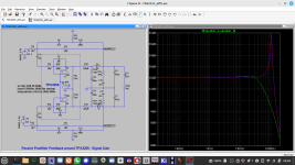
Schematic:

Frequency and phase repsonse:

Fourier graph for 0dB input level (155 mVrms):

Fourier graph for ~ -3dB input level (110 mVrms):

Fourier graph for ~ -6dB input level (78 mVrms):

I know that this tube-related digression deviates from the topic of the subforum, but ultimately, it is intended to be a hybrid of a tube and Class D. In my opinion, it should be mentioned in this post, where I hope a discussion will take place. I am essentially a beginner hobbyist in electronics, so I would gladly read comments from someone who may have worked on PFFB loops for the TPA3244/45/50/51/55 chips.
PS:
Setpoint of V1: Uak = 34.0 V, Ia = 2.28 mA, Ugk = -1.28 V.
Setpoint of V2: Uak = 40.0 V, Ia = 1.31 mA, Ugk = -2.10 V.
Supply voltage after R10: 73.6 V.
Simulations were done using TINA, which has its pros and cons; unfortunately, a major downside is the relatively high level of THD-N for higher harmonics with small signals. That’s why I provided the harmonic distribution for the level of 0dB (full modulation with a margin of 6dB) as well as -3dB and 6dB. This problem with the high level of higher harmonics in the Fourier analysis essentially makes it pointless to show simulations for lower levels of modulation, as those harmonics disappear. The analysis practically shows a constant value of harmonics starting from the third harmonic. We have thus the desired dominance of the second harmonic (and a few my practical implementations confirm the nature of the harmonic distribution).
Limiting the bandwidth on high frequenies additionally increases the attenuation of ripple when we power the tube stages from a converter. However, note that if we do not frequency-compensate the voltage regulation loop, they will "buzz" in the range from several hundred Hz to a few kHz, even though the switching frequency of the converter is above 0.5 MHz and around 2 MHz. Care must be taken with low loads and we should use a capacitor at the output with a relatively large capacitance and low ESR.
Schematic:
Frequency and phase repsonse:
Fourier graph for 0dB input level (155 mVrms):
Fourier graph for ~ -3dB input level (110 mVrms):
Fourier graph for ~ -6dB input level (78 mVrms):
I know that this tube-related digression deviates from the topic of the subforum, but ultimately, it is intended to be a hybrid of a tube and Class D. In my opinion, it should be mentioned in this post, where I hope a discussion will take place. I am essentially a beginner hobbyist in electronics, so I would gladly read comments from someone who may have worked on PFFB loops for the TPA3244/45/50/51/55 chips.
PS:
Setpoint of V1: Uak = 34.0 V, Ia = 2.28 mA, Ugk = -1.28 V.
Setpoint of V2: Uak = 40.0 V, Ia = 1.31 mA, Ugk = -2.10 V.
Supply voltage after R10: 73.6 V.
Last edited:
Hey Studi,
That one seems quite interesting. Do you plan to experiment with the PFFB Values?
there is a lack of material on actual proven values with different parameters here 😀
That one seems quite interesting. Do you plan to experiment with the PFFB Values?
there is a lack of material on actual proven values with different parameters here 😀
Could not wait, so I updated my simulation file according to yours.
Frequency response is indeed excellent -
as long as your load is non-inductive.
In real life there are series inductance that give a peak around 100kHz.
Nonetheless frequency response in the audio band remains excellent.
Besides these components are superfluous:
R11, C12, R2, C4, R16, C13, R17, C14
Frequency response is indeed excellent -
as long as your load is non-inductive.
In real life there are series inductance that give a peak around 100kHz.
Nonetheless frequency response in the audio band remains excellent.
Besides these components are superfluous:
R11, C12, R2, C4, R16, C13, R17, C14
Attachments
Hello, first, a few words of explanation. Currently, I am experiencing some disruptions regarding my professional work, so any attempts to create a working prototype, measure it, and test it will have to be postponed to the future (more likely May/June rather than February/March). For now, I can only present the results of the analysis of the documentation for products by Texas Instruments (Burr-Brown) from the group of Class D audio amplifiers with an analog input.
I started this thread with the idea of a hybrid design, namely a tube-based preamplifier stage combined with a Class D power amplifier stage. In this initial approach, I selected the TPA3245 / TPA3251 chips (I dismissed the TPA3244 / TPA3250 models due to the thermal pad located on the underside of the integrated circuit package, which prevents the use of a heatsink). What favored this family of chips was the published ready-made solution for an additional PFF (post-filter feedback) loop that encompasses the output LC reconstruction filters (second-order).
A drawback of choosing this series is, first and foremost, the lack of any SPICE model. Attempting simplified modeling in SPICE has certain limitations since it would not replicate the amplitude-frequency characteristics of this system. Such characteristics are essential when modeling an object enclosed within an additional negative feedback loop that also encompasses the LC elements. Without this, the results would be inaccurate. Another argument against this series is that I do not require high output power. The speaker impedances are definitively 8 ohms rather than 4 ohms.
Furthermore, when using an additional negative feedback loop, it is preferable for the object within this loop to have high gain. With low gain, the achievable depth of the additional negative feedback loop will be relatively shallow. This means the expected reduction in distortion caused by the cores of the output inductors in the reconstruction filters will be limited. Texas Instruments’ publication describing the PFF loop for this series of Class D power amplifiers demonstrates that the depth of the PFF loop is only about 6 dB, resulting in only a roughly twofold improvement in THD figures.
The only significant advantage would be the reduction of ringing in the LC filters, as the same THD improvement could be achieved by using better inductors. This is particularly straightforward in cases like mine, where the power requirements are modest (approximately 33–35 W for 8-ohm loads). The TPA3245 has a gain of 18 dB, while the TPA3251 has a gain of 20 dB. After applying the additional PFF loop, the gain drops to around 12–14 dB, meaning a higher input signal amplitude is required. For me, this is a drawback, as I intend to add a tube-based preamp stage but prefer to avoid using high anode voltages. To avoid complicating the DC/DC converters, there is a limit of 60V for anode voltages. This implies that it would be advantageous for the power stage to have higher gain.
After further consideration, my choice falls on the TPA3126 and TPA3156 chips, which are improved evolutionary versions of the TPA3116. These chips offer slightly better THD performance, improved energy efficiency, and employ a modified modulation scheme designed for applications where power consumption is a critical parameter (which is not a requirement for me, as my amplifier will not be battery-powered). The TPA3156 chip can deliver higher output currents, eliminating the limitation on maximum supply voltage for a 4-ohm load, which is 21V instead of 26V. If we plan to use a 4-ohm load, the TPA3156 is the appropriate choice, while for 8-ohm loads, the TPA3126 is sufficient.
It’s worth mentioning the topic of heatsinks at this point. I want to avoid, especially at the prototype stage, ordering a custom heatsink profile. I do not accept adhesive heatsinks, like those used by some Chinese manufacturers, as they are subpar—prone to detachment and characterized by high thermal resistance between the power/thermal pad and the heatsink surface.
For their EVM boards, Texas Instruments ordered dedicated heatsinks from Advanced Thermal Solutions. Since I am planning for an 8-ohm load and will settle for a 24V power supply, the heatsink used on the TPA3116 EVM boards would also suffice for the TPA3245/TPA3251 chips. Unfortunately, the heatsinks for these more powerful chips are quite large, which I consider a disadvantage because they increase the length of critical traces between the chips and the electrolytic capacitors providing power decoupling. The heatsinks designed for the TPA3116 EVM boards can be used with TPA3245/TPA3251 chips, provided the load impedance is 4 or 8 ohms and the supply voltage does not exceed 26V. That concludes my digression on heatsinks. Let’s move on.
Before discussing the amplifier project with the TPA3126 chip and a PFF loop, I need to address the matter of clock frequency. Lower-power chips like the TPA3116, TPA3126, and TPA3156 allow for switching frequencies of up to 1200kHz. I do not agree with the opinion that 400kHz is sufficient. It is not, because the cutoff frequency of the LC filters should be no higher than 40kHz (1/10 of the switching frequency). This is too close to the upper end of the audio spectrum, and such an LC filter will inevitably affect the frequency response, particularly causing significant phase shift.
The second argument against 400kHz is evident: when sampling an analog signal to produce a pulse waveform, the higher the switching frequency, the more accurately high frequencies can be reproduced. Unfortunately, datasheets typically report performance metrics for a 400kHz switching frequency. However, upon exploring Texas Instruments' resources, one can find data for the TPA6304 chip, which details THD performance for switching frequencies of 384kHz and 2100kHz under two different modulation schemes. The relevant graphs below illustrate this clearly.
Let’s proceed to analyze these findings.
TPA6304, 384kHz:

TPA6304, 2100kHz:

To provide a comparison, below is a similar graph for the TPA3126 chip, showing its performance with a 400kHz switching frequency and Hybrid modulation:

The conclusions, which in my opinion are straightforward, I leave to you, the readers of this thread. I have chosen a switching frequency of 1200kHz. This allows the design of output LC reconstruction filters with a higher cutoff frequency of approximately 107kHz. Additionally, I can select the components of the PFF loop, which shape the frequency response, to have a higher characteristic frequency than those presented by Texas Instruments for the TPA3245 / TPA3251 chips. This means that at 20kHz, I will achieve less phase shift, which is also desirable. Furthermore, the higher switching frequency provides more "headroom" for the LC filter characteristics. I opted for an inductance of 10µH and a capacitance of 220nF, even though a 7µH inductance would have been a better choice. However, I already have inductors with a 10µH value, which I will discuss further later.
Here is the design.

I implemented a PFF loop with greater depth than that described in the Texas Instruments publication. I selected a gain of 26dB for the TPA3126 chip. Using resistors in the PFF loop with values of 18k / 2k7 (as in the publication), the PFF loop depth is 11.6dB (a 3.8-fold reduction in THD), and the power stage gain is 14.4dB. For 18k / 3k3, the corresponding values are 13.9dB (4.9-fold reduction in THD) and 12.1dB, and for 18k / 3k9, the values are 15.0dB (5.7-fold reduction in THD) and 11.0dB. It is evident what the increased system gain of 26dB (as opposed to 18dB) provides: instead of an approximately twofold reduction in THD, we achieve nearly a fourfold reduction.The complete system includes a phase inverter and a preamp stage, where a first-order high-pass filter must be implemented.
One more thing, which an observant reader may have already noticed: the PFF loops are implemented "crosswise." Yes, the TPA3116, TPA3126, and TPA3156 chips have four channels that do not invert the phase, unlike the TPA3244, TPA3245, TPA3250, TPA3251, TPA3220, TPA3221, and TPA3223 chips, which are based on a higher-power series design.
In these lower-power chips, the positive input is connected to the loop from the negative output (each stereo channel consists of two amplification paths working as a balanced symmetric circuit). The second element is the phase inverter, which is essential. The requirement for low output impedance was the deciding factor to implement it "in silicon" rather than using tubes. Cathode followers on the inverter's output with shared load would require multiplying the number of tubes, which are becoming increasingly expensive and difficult to find.
In my opinion, only a single tube pre-stage is sufficient, which provides the tube-like coloration by adding the second harmonic. For the phase inverters, I selected the OPA862 chips, whose internal structure is shown in the provided schematic. While these are somewhat more expensive than using typical operational amplifiers, they involve fewer components, are simpler, and take up less PCB layout space. The tube pre-stage doesn’t need further explanation. The required high-pass filter is implemented with a capacitor between the anode and ground, which also helps to suppress ripple coming from the power supply providing the anode voltage. For the tube, I chose the Soviet-made 6S51N-V nuwistor (military-grade). These Soviet nuwistors are slightly modified from the originals, with long and flexible wire leads that facilitate direct mounting onto the PCB without needing sockets or cutting the side keys in the metal housing of the original nuwistors.
I could suggest using another Soviet nuwistor, the 6S63N, which is a bit more exotic but still available. Other subminiature glass tubes include interesting hybrids of frame-grid and rod-type tubes, such as the 6N28N-C dual triode and the 6SH45B-V pentode.
For the 6S51N-V tube stage, using 18k/2k7 resistors in the PFF loop, the gain is 33.8dB (49-fold reduction), with 18k/3k3 it’s 32.4dB (42-fold reduction), and with 18k/3k9 it’s 31.2dB (36-fold reduction). The gain is defined as Vpp / Vi (where Vpp refers to the peak-to-peak output voltage of the balanced output, and Vi refers to the peak input voltage of the unbalanced input).
I should mention that this might be too much gain, but in practice, a sensitivity of around 1Vp might not be enough. A slightly lower input signal amplitude is desirable to avoid generating the third harmonic at the output of the tube pre-stage. The sensitivities resulting from the gain and the output power limited by the 24V supply voltage fall within the range of 335mVrms to 445mVrms.
Lastly, a word about the inductors: I’m referring to specially designed double inductors, which are not coupled together, even though they are placed within the same closed core that provides shielding. The manufacturer is Coilcraft, with the model UA8104-AL (the 7uH version is UAL8103-AL). These inductors look promising, as Texas Instruments has published comparative THD performance with other inductors:
https://www.ti.com/lit/an/slaa701a/slaa701a.pdf?ts=1736749519432
Here are the results of the simulations. First, I present the amplitude-frequency and phase-frequency characteristics for 8Ω and 4Ω load conditions:

The next issue is the problem of no load, where a 2.2kΩ resistor becomes the load for the amplifier. To demonstrate how the system behaves, I show the waveforms for a square wave signal:

Next, I present the key switching frequency attenuation, which is 42dB, a very good result. Attached are additional amplitude-frequency and phase-frequency characteristics, which provide a comprehensive view of the system's ringing behavior, high-frequency performance, and the suppression of the carrier frequency.

At this point, I’d like to point out that there are no classic Zobel networks; instead, I use a pair of RC snubbers before and after the LC filter. These snubbers help reduce radio frequency interference emissions. It is interesting to see the response to a square wave signal before these filters are applied.

Finally, I present the estimated Total Harmonic Distortion (THD) of the entire amplifier.
Input level 0dB (max output power before clipping):

Input level -3dB:

Input level -6dB:

Input level -10dB:

Input level -16dB:

Input level -20dB:

In the next post, I will share the prototype design.
I started this thread with the idea of a hybrid design, namely a tube-based preamplifier stage combined with a Class D power amplifier stage. In this initial approach, I selected the TPA3245 / TPA3251 chips (I dismissed the TPA3244 / TPA3250 models due to the thermal pad located on the underside of the integrated circuit package, which prevents the use of a heatsink). What favored this family of chips was the published ready-made solution for an additional PFF (post-filter feedback) loop that encompasses the output LC reconstruction filters (second-order).
A drawback of choosing this series is, first and foremost, the lack of any SPICE model. Attempting simplified modeling in SPICE has certain limitations since it would not replicate the amplitude-frequency characteristics of this system. Such characteristics are essential when modeling an object enclosed within an additional negative feedback loop that also encompasses the LC elements. Without this, the results would be inaccurate. Another argument against this series is that I do not require high output power. The speaker impedances are definitively 8 ohms rather than 4 ohms.
Furthermore, when using an additional negative feedback loop, it is preferable for the object within this loop to have high gain. With low gain, the achievable depth of the additional negative feedback loop will be relatively shallow. This means the expected reduction in distortion caused by the cores of the output inductors in the reconstruction filters will be limited. Texas Instruments’ publication describing the PFF loop for this series of Class D power amplifiers demonstrates that the depth of the PFF loop is only about 6 dB, resulting in only a roughly twofold improvement in THD figures.
The only significant advantage would be the reduction of ringing in the LC filters, as the same THD improvement could be achieved by using better inductors. This is particularly straightforward in cases like mine, where the power requirements are modest (approximately 33–35 W for 8-ohm loads). The TPA3245 has a gain of 18 dB, while the TPA3251 has a gain of 20 dB. After applying the additional PFF loop, the gain drops to around 12–14 dB, meaning a higher input signal amplitude is required. For me, this is a drawback, as I intend to add a tube-based preamp stage but prefer to avoid using high anode voltages. To avoid complicating the DC/DC converters, there is a limit of 60V for anode voltages. This implies that it would be advantageous for the power stage to have higher gain.
After further consideration, my choice falls on the TPA3126 and TPA3156 chips, which are improved evolutionary versions of the TPA3116. These chips offer slightly better THD performance, improved energy efficiency, and employ a modified modulation scheme designed for applications where power consumption is a critical parameter (which is not a requirement for me, as my amplifier will not be battery-powered). The TPA3156 chip can deliver higher output currents, eliminating the limitation on maximum supply voltage for a 4-ohm load, which is 21V instead of 26V. If we plan to use a 4-ohm load, the TPA3156 is the appropriate choice, while for 8-ohm loads, the TPA3126 is sufficient.
It’s worth mentioning the topic of heatsinks at this point. I want to avoid, especially at the prototype stage, ordering a custom heatsink profile. I do not accept adhesive heatsinks, like those used by some Chinese manufacturers, as they are subpar—prone to detachment and characterized by high thermal resistance between the power/thermal pad and the heatsink surface.
For their EVM boards, Texas Instruments ordered dedicated heatsinks from Advanced Thermal Solutions. Since I am planning for an 8-ohm load and will settle for a 24V power supply, the heatsink used on the TPA3116 EVM boards would also suffice for the TPA3245/TPA3251 chips. Unfortunately, the heatsinks for these more powerful chips are quite large, which I consider a disadvantage because they increase the length of critical traces between the chips and the electrolytic capacitors providing power decoupling. The heatsinks designed for the TPA3116 EVM boards can be used with TPA3245/TPA3251 chips, provided the load impedance is 4 or 8 ohms and the supply voltage does not exceed 26V. That concludes my digression on heatsinks. Let’s move on.
Before discussing the amplifier project with the TPA3126 chip and a PFF loop, I need to address the matter of clock frequency. Lower-power chips like the TPA3116, TPA3126, and TPA3156 allow for switching frequencies of up to 1200kHz. I do not agree with the opinion that 400kHz is sufficient. It is not, because the cutoff frequency of the LC filters should be no higher than 40kHz (1/10 of the switching frequency). This is too close to the upper end of the audio spectrum, and such an LC filter will inevitably affect the frequency response, particularly causing significant phase shift.
The second argument against 400kHz is evident: when sampling an analog signal to produce a pulse waveform, the higher the switching frequency, the more accurately high frequencies can be reproduced. Unfortunately, datasheets typically report performance metrics for a 400kHz switching frequency. However, upon exploring Texas Instruments' resources, one can find data for the TPA6304 chip, which details THD performance for switching frequencies of 384kHz and 2100kHz under two different modulation schemes. The relevant graphs below illustrate this clearly.
Let’s proceed to analyze these findings.
TPA6304, 384kHz:
TPA6304, 2100kHz:
To provide a comparison, below is a similar graph for the TPA3126 chip, showing its performance with a 400kHz switching frequency and Hybrid modulation:
The conclusions, which in my opinion are straightforward, I leave to you, the readers of this thread. I have chosen a switching frequency of 1200kHz. This allows the design of output LC reconstruction filters with a higher cutoff frequency of approximately 107kHz. Additionally, I can select the components of the PFF loop, which shape the frequency response, to have a higher characteristic frequency than those presented by Texas Instruments for the TPA3245 / TPA3251 chips. This means that at 20kHz, I will achieve less phase shift, which is also desirable. Furthermore, the higher switching frequency provides more "headroom" for the LC filter characteristics. I opted for an inductance of 10µH and a capacitance of 220nF, even though a 7µH inductance would have been a better choice. However, I already have inductors with a 10µH value, which I will discuss further later.
Here is the design.
I implemented a PFF loop with greater depth than that described in the Texas Instruments publication. I selected a gain of 26dB for the TPA3126 chip. Using resistors in the PFF loop with values of 18k / 2k7 (as in the publication), the PFF loop depth is 11.6dB (a 3.8-fold reduction in THD), and the power stage gain is 14.4dB. For 18k / 3k3, the corresponding values are 13.9dB (4.9-fold reduction in THD) and 12.1dB, and for 18k / 3k9, the values are 15.0dB (5.7-fold reduction in THD) and 11.0dB. It is evident what the increased system gain of 26dB (as opposed to 18dB) provides: instead of an approximately twofold reduction in THD, we achieve nearly a fourfold reduction.The complete system includes a phase inverter and a preamp stage, where a first-order high-pass filter must be implemented.
One more thing, which an observant reader may have already noticed: the PFF loops are implemented "crosswise." Yes, the TPA3116, TPA3126, and TPA3156 chips have four channels that do not invert the phase, unlike the TPA3244, TPA3245, TPA3250, TPA3251, TPA3220, TPA3221, and TPA3223 chips, which are based on a higher-power series design.
In these lower-power chips, the positive input is connected to the loop from the negative output (each stereo channel consists of two amplification paths working as a balanced symmetric circuit). The second element is the phase inverter, which is essential. The requirement for low output impedance was the deciding factor to implement it "in silicon" rather than using tubes. Cathode followers on the inverter's output with shared load would require multiplying the number of tubes, which are becoming increasingly expensive and difficult to find.
In my opinion, only a single tube pre-stage is sufficient, which provides the tube-like coloration by adding the second harmonic. For the phase inverters, I selected the OPA862 chips, whose internal structure is shown in the provided schematic. While these are somewhat more expensive than using typical operational amplifiers, they involve fewer components, are simpler, and take up less PCB layout space. The tube pre-stage doesn’t need further explanation. The required high-pass filter is implemented with a capacitor between the anode and ground, which also helps to suppress ripple coming from the power supply providing the anode voltage. For the tube, I chose the Soviet-made 6S51N-V nuwistor (military-grade). These Soviet nuwistors are slightly modified from the originals, with long and flexible wire leads that facilitate direct mounting onto the PCB without needing sockets or cutting the side keys in the metal housing of the original nuwistors.
I could suggest using another Soviet nuwistor, the 6S63N, which is a bit more exotic but still available. Other subminiature glass tubes include interesting hybrids of frame-grid and rod-type tubes, such as the 6N28N-C dual triode and the 6SH45B-V pentode.
For the 6S51N-V tube stage, using 18k/2k7 resistors in the PFF loop, the gain is 33.8dB (49-fold reduction), with 18k/3k3 it’s 32.4dB (42-fold reduction), and with 18k/3k9 it’s 31.2dB (36-fold reduction). The gain is defined as Vpp / Vi (where Vpp refers to the peak-to-peak output voltage of the balanced output, and Vi refers to the peak input voltage of the unbalanced input).
I should mention that this might be too much gain, but in practice, a sensitivity of around 1Vp might not be enough. A slightly lower input signal amplitude is desirable to avoid generating the third harmonic at the output of the tube pre-stage. The sensitivities resulting from the gain and the output power limited by the 24V supply voltage fall within the range of 335mVrms to 445mVrms.
Lastly, a word about the inductors: I’m referring to specially designed double inductors, which are not coupled together, even though they are placed within the same closed core that provides shielding. The manufacturer is Coilcraft, with the model UA8104-AL (the 7uH version is UAL8103-AL). These inductors look promising, as Texas Instruments has published comparative THD performance with other inductors:
https://www.ti.com/lit/an/slaa701a/slaa701a.pdf?ts=1736749519432
Here are the results of the simulations. First, I present the amplitude-frequency and phase-frequency characteristics for 8Ω and 4Ω load conditions:
The next issue is the problem of no load, where a 2.2kΩ resistor becomes the load for the amplifier. To demonstrate how the system behaves, I show the waveforms for a square wave signal:
Next, I present the key switching frequency attenuation, which is 42dB, a very good result. Attached are additional amplitude-frequency and phase-frequency characteristics, which provide a comprehensive view of the system's ringing behavior, high-frequency performance, and the suppression of the carrier frequency.
At this point, I’d like to point out that there are no classic Zobel networks; instead, I use a pair of RC snubbers before and after the LC filter. These snubbers help reduce radio frequency interference emissions. It is interesting to see the response to a square wave signal before these filters are applied.
Finally, I present the estimated Total Harmonic Distortion (THD) of the entire amplifier.
Input level 0dB (max output power before clipping):
Input level -3dB:
Input level -6dB:
Input level -10dB:
Input level -16dB:
Input level -20dB:
In the next post, I will share the prototype design.
Last edited:
The prototype design, which is meant to verify the theoretical considerations in SPICE.
Schematic diagram:

PCB design, top side:

PCB design, bottom side:

PCB render, top side:

PCB render, bottom side:

DC/DC converter simulations in PDF files.
General description.
As can be seen, there will be two switched inputs. The power is switched via a relay, but I would like to point out that traditional relays, even those labeled as high-inrush, are not suitable. A pre-make tungsten relay with a normally closed contact will be used, as only such a relay will not stick due to the low ESR value of the decoupling capacitors (these are organic, polymer capacitors). The input stages and phase inverters have their own signal grounds, implemented in a star topology. The ground of the power supply is separated from the power stage ground and the ground filling the PCB area. The anode voltage converter has additional load because, for low current draw with high output capacitance and low ESR of the output capacitor, it is difficult to maintain the stability of the voltage regulation loop (the converter may start oscillating at an audible frequency). The lamp filaments are connected in series. For powering the OPA862 (10V), an LDO regulator with high ripple rejection is used. This regulator is powered from the lamp filament supply. A delayed output activation circuit is essential, and I used the _MUTE signal from the control circuit. The appropriate delay is implemented with a simple and effective circuit based on a single transistor and a low-signal relay. During power-on and when the power is lost, voltage spikes (positive during power-on and negative during power loss) can reach the inputs of the OPA862. The OPA862 circuits have diodes integrated in their structure to protect against such surges, but I added additional Schottky diodes for extra protection.
C1L, C1R, C4L, C4R, C9L, C9R, C10L, C10R - MKS2 film capacitors (metallized polyester).
C17L, C17R, C18L, C18R - MKP2 film capacitors (metallized polypropylene).
C2L, C2R, C11L - C16L, C11R - C16R, C19L, C19R, C20L, C20R, C24L, C24R - MLCC C0G capacitors.
C5L, C5R, C7L, C7R, C36 - MLCC U2J capacitors.
C21L, C21R, C22L, C22R - MLCC U2J or X7R capacitors
C37 - polymer tantalum capacitor.
C38 - aluminium electrolyctic capacitor.
All other electrolyctic capacitors are aluminium organic polymer capacitors.
Other non-electrolyctic capacitors are MLSS X7R capacitors.
R1L - R16L, R1R - R16R, R17L, R17R, R18L, R18R - MELF 0204 resitors.
R17L - R19L, R17R - R19R - MELF 0207 resistors.
L1, L3, L4, L5 - Coilcraft MSS7348 inductors.
L2L, L2R - Coilcraft UA8104-AL inductors.
L6 - Coilcraft MSS1260 inductor.
L7 - Coilcraft MSS1210 inductor.
Best regards to those reading, and I’m waiting for the bucket of criticism to be poured over my head. 😉
PS: A small clarification to the previous post: the characteristics additionally describing the filter attenuation: Uoic refers to the waveforms before the LC filters, and Uo refers to the waveforms after the LC filters.
Schematic diagram:
PCB design, top side:
PCB design, bottom side:
PCB render, top side:
PCB render, bottom side:
DC/DC converter simulations in PDF files.
General description.
As can be seen, there will be two switched inputs. The power is switched via a relay, but I would like to point out that traditional relays, even those labeled as high-inrush, are not suitable. A pre-make tungsten relay with a normally closed contact will be used, as only such a relay will not stick due to the low ESR value of the decoupling capacitors (these are organic, polymer capacitors). The input stages and phase inverters have their own signal grounds, implemented in a star topology. The ground of the power supply is separated from the power stage ground and the ground filling the PCB area. The anode voltage converter has additional load because, for low current draw with high output capacitance and low ESR of the output capacitor, it is difficult to maintain the stability of the voltage regulation loop (the converter may start oscillating at an audible frequency). The lamp filaments are connected in series. For powering the OPA862 (10V), an LDO regulator with high ripple rejection is used. This regulator is powered from the lamp filament supply. A delayed output activation circuit is essential, and I used the _MUTE signal from the control circuit. The appropriate delay is implemented with a simple and effective circuit based on a single transistor and a low-signal relay. During power-on and when the power is lost, voltage spikes (positive during power-on and negative during power loss) can reach the inputs of the OPA862. The OPA862 circuits have diodes integrated in their structure to protect against such surges, but I added additional Schottky diodes for extra protection.
C1L, C1R, C4L, C4R, C9L, C9R, C10L, C10R - MKS2 film capacitors (metallized polyester).
C17L, C17R, C18L, C18R - MKP2 film capacitors (metallized polypropylene).
C2L, C2R, C11L - C16L, C11R - C16R, C19L, C19R, C20L, C20R, C24L, C24R - MLCC C0G capacitors.
C5L, C5R, C7L, C7R, C36 - MLCC U2J capacitors.
C21L, C21R, C22L, C22R - MLCC U2J or X7R capacitors
C37 - polymer tantalum capacitor.
C38 - aluminium electrolyctic capacitor.
All other electrolyctic capacitors are aluminium organic polymer capacitors.
Other non-electrolyctic capacitors are MLSS X7R capacitors.
R1L - R16L, R1R - R16R, R17L, R17R, R18L, R18R - MELF 0204 resitors.
R17L - R19L, R17R - R19R - MELF 0207 resistors.
L1, L3, L4, L5 - Coilcraft MSS7348 inductors.
L2L, L2R - Coilcraft UA8104-AL inductors.
L6 - Coilcraft MSS1260 inductor.
L7 - Coilcraft MSS1210 inductor.
Best regards to those reading, and I’m waiting for the bucket of criticism to be poured over my head. 😉
PS: A small clarification to the previous post: the characteristics additionally describing the filter attenuation: Uoic refers to the waveforms before the LC filters, and Uo refers to the waveforms after the LC filters.
Attachments
Last edited:
In my opinion, it is better to use the SPICE models of the TPA3126 circuits published by Texas Instruments. Unfortunately, these models are encrypted and only available for TINA (which is a free tool). These models, offering full small-signal analysis (the model responds to the choice of clock frequency) and limited transient analysis, will provide better results than simplified modeling, as we do not know the real structure of these circuits and, consequently, the filtering in the analog signal path and its order. As for the conversion of the analog signal to pulses by the comparators, Nyquist’s theorem can be applied.@STUDI would you mind publishing your asc-file here so other members can play with your simulation.
btw, if 10W/8Ohms fit your bill you might consider TPA3118.
Encrypted SPICE model of TPA3126 in attachments. This model is published by Texas Instruments.
SPICE models - electron tubes:
Subminiature frame-grid / rode, military pentode from Soviet-Union 6SH45-V / 6J45B-V (6Ж45Б-В):
****************************************************
.SUBCKT 6J45B-V_p 1 2 3 4 ; Plate Screen Grid Cathode
PARAMS: MU= 27.77 EX=1.226 kG1=143.4 KP=105.1 kVB=402.0 kG2=2549.0
Sc=0.14E+02 ap=0.100 w=11.0 nu=0.00 lam=296554.4
Ookg1mOokG2=0.658E-02 Aokg1=0.52E-11 alkg1palskg2=0.658E-02 be=14.622 als=12.22 RGI=2000
CCG1=6.1P CCG2 = 3.7p CPG1 = 0.05p CG1G2 = 3.7p CCP=2.3P
****************************************************
RE1 7 0 1MEG ; DUMMY SO NODE 7 HAS 2 CONNECTIONS
E1 7 0 VALUE=
+{V(2,4)/KP*LOG(1+EXP(KP*(1/MU+V(3,4)/SQRT(KVB+V(2,4)*V(2,4)))))}
E2 8 0 VALUE = {Ookg1mOokG2 + Aokg1*V(1,4) - alkg1palskg2/(1+be*V(1,4)/V(2,4))}
E3 9 0 VALUE = {Sc/kG2*V(1,4)(1+tanh(-ap(V(1,4)-V(2,4)/lam+w+nu*V(3,4))))}
G1 1 4 VALUE = {0.5*(PWR(V(7),EX)+PWRS(V(7),EX))*(V(8)-V(9))}
G2 2 4 VALUE = {0.5*(PWR(V(7),EX)+PWRS(V(7),EX))/KG2 * (1+ als/(1+be*V(1,4)/V(2,4)))}
RCP 1 4 1G ; FOR CONVERGENCE A - C
C1 3 4 {CCG1} ; CATHODE-GRID 1 C - G1
C4 2 4 {CCG2} ; CATHODE-GRID 2 C - G2
C5 2 3 {CG1G2} ; GRID 1 -GRID 2 G1 - G2
C2 1 3 {CPG1} ; GRID 1-PLATE G1 - A
C3 1 4 {CCP} ; CATHODE-PLATE A - C
R1 3 5 {RGI} ; FOR GRID CURRENT G1 - 5
D3 5 4 DX ; FOR GRID CURRENT 5 - C
.MODEL DX D(IS=1N RS=1 CJO=10PF TT=1N)
.ENDS
Subminiature frame-grid / rode, military pentode from Soviet-Union 6SH45-V / 6J45B-V (6Ж45Б-В) connected as triode:
****************************************************
.SUBCKT 6J45B-V_t 1 2 3; A G C
PARAMS: MU=27.77 EX=1.226 KG1=143.4 KP=105.1 KVB=402.0 RGI=2000
CCG=6.1P CGP=4.5P CCP=4.0P
****************************************************
E1 7 0 VALUE=
+{V(1,3)/KP*LOG(1+EXP(KP*(1/MU+V(2,3)/SQRT(KVB+V(1,3)*V(1,3)))))}
RE1 7 0 1G
G1 1 3 VALUE={0.5*(PWR(V(7),EX)+PWRS(V(7),EX))/KG1}
RCP 1 3 1G ; TO AVOID FLOATING NODES IN MU-FOLLOWER
C1 2 3 {CCG} ; CATHODE-GRID
C2 2 1 {CGP} ; GRID-PLATE
C3 1 3 {CCP} ; CATHODE-PLATE
D3 5 3 DX ; FOR GRID CURRENT
R1 2 5 {RGI} ; FOR GRID CURRENT
.MODEL DX D(IS=1N RS=1 CJO=10PF TT=1N)
.ENDS


Subminiature frame-grid / rode, military duotriode from Soviet-Union 6N28N-V (6Н28Б-В):
****************************************************
.SUBCKT 6N28B-V_t 1 2 3; A G C
PARAMS: MU=23.10 EX=1.149 KG1=184.2 KP=121.1 KVB=417.0 RGI=2000
CCG=3.3P CGP=2.0P CCP=2.2P
****************************************************
E1 7 0 VALUE=
+{V(1,3)/KP*LOG(1+EXP(KP*(1/MU+V(2,3)/SQRT(KVB+V(1,3)*V(1,3)))))}
RE1 7 0 1G
G1 1 3 VALUE={0.5*(PWR(V(7),EX)+PWRS(V(7),EX))/KG1}
RCP 1 3 1G ; TO AVOID FLOATING NODES IN MU-FOLLOWER
C1 2 3 {CCG} ; CATHODE-GRID
C2 2 1 {CGP} ; GRID-PLATE
C3 1 3 {CCP} ; CATHODE-PLATE
D3 5 3 DX ; FOR GRID CURRENT
R1 2 5 {RGI} ; FOR GRID CURRENT
.MODEL DX D(IS=1N RS=1 CJO=10PF TT=1N)
.ENDS
Subminiature frame-grid / rode, military duotriode from Soviet-Union 6N28N-V (6Н28Б-В) - parallel conceted triode systems:
****************************************************
.SUBCKT 6N28B-V_2t 1 2 3; A G C
PARAMS: MU=21.15 EX=1.191 KG1=101.8 KP=129.4 KVB=445.0 RGI=2000
CCG=6.6P CGP=4.4P CCP=4.0P
****************************************************
E1 7 0 VALUE=
+{V(1,3)/KP*LOG(1+EXP(KP*(1/MU+V(2,3)/SQRT(KVB+V(1,3)*V(1,3)))))}
RE1 7 0 1G
G1 1 3 VALUE={0.5*(PWR(V(7),EX)+PWRS(V(7),EX))/KG1}
RCP 1 3 1G ; TO AVOID FLOATING NODES IN MU-FOLLOWER
C1 2 3 {CCG} ; CATHODE-GRID
C2 2 1 {CGP} ; GRID-PLATE
C3 1 3 {CCP} ; CATHODE-PLATE
D3 5 3 DX ; FOR GRID CURRENT
R1 2 5 {RGI} ; FOR GRID CURRENT
.MODEL DX D(IS=1N RS=1 CJO=10PF TT=1N)
.ENDS
Nuvistor military triode from Soviet-Union 6S51N-V (6С51Н-В):
****************************************************
.SUBCKT 6S51N-V_LV 1 2 3 ; Plate Grid Cathode
PARAMS: CCG=4.6P CGP=1.7P CCP=2P RGI=2000
MU=37.07 KG1=196.88 KP=102.48 KVB=254.1 VCT=0.1004 EX=1.343
****************************************************
E1 7 0 VALUE={V(1,3)/KP*LOG(1+EXP(KP*(1/MU+(VCT+V(2,3))/SQRT(KVB+V(1,3)*V(1,3)))))}
RE1 7 0 1G ; TO AVOID FLOATING NODES
G1 1 3 VALUE={(PWR(V(7),EX)+PWRS(V(7),EX))/KG1}
RCP 1 3 1G ; TO AVOID FLOATING NODES
C1 2 3 {CCG} ; CATHODE-GRID
C2 2 1 {CGP} ; GRID=PLATE
C3 1 3 {CCP} ; CATHODE-PLATE
D3 5 3 DX ; POSITIVE GRID CURRENT
R1 2 5 {RGI} ; POSITIVE GRID CURRENT
.MODEL DX D(IS=1N RS=1 CJO=10PF TT=1N)
.ENDS
*$

Nuvistor low-voltage triode from Soviet-Union 6S63N (6С63Н):
****************************************************
.SUBCKT 6S63N_LV 1 2 3 ; Plate Grid Cathode
PARAMS: CCG=4.6P CGP=2.2P CCP=2.5P RGI=2000
MU=12.9 KG1=265.5 KP=38.58 KVB=61.5 VCT=0.06318 EX=1.121
****************************************************
E1 7 0 VALUE={V(1,3)/KP*LOG(1+EXP(KP*(1/MU+(VCT+V(2,3))/SQRT(KVB+V(1,3)*V(1,3)))))}
RE1 7 0 1G ; TO AVOID FLOATING NODES
G1 1 3 VALUE={(PWR(V(7),EX)+PWRS(V(7),EX))/KG1}
RCP 1 3 1G ; TO AVOID FLOATING NODES
C1 2 3 {CCG} ; CATHODE-GRID
C2 2 1 {CGP} ; GRID=PLATE
C3 1 3 {CCP} ; CATHODE-PLATE
D3 5 3 DX ; POSITIVE GRID CURRENT
R1 2 5 {RGI} ; POSITIVE GRID CURRENT
.MODEL DX D(IS=1N RS=1 CJO=10PF TT=1N)
.ENDS
*$

PS: My mistakes: Coilcraft UA8014-AL UA8013-AL.
SPICE models - electron tubes:
Subminiature frame-grid / rode, military pentode from Soviet-Union 6SH45-V / 6J45B-V (6Ж45Б-В):
****************************************************
.SUBCKT 6J45B-V_p 1 2 3 4 ; Plate Screen Grid Cathode
PARAMS: MU= 27.77 EX=1.226 kG1=143.4 KP=105.1 kVB=402.0 kG2=2549.0
Sc=0.14E+02 ap=0.100 w=11.0 nu=0.00 lam=296554.4
Ookg1mOokG2=0.658E-02 Aokg1=0.52E-11 alkg1palskg2=0.658E-02 be=14.622 als=12.22 RGI=2000
CCG1=6.1P CCG2 = 3.7p CPG1 = 0.05p CG1G2 = 3.7p CCP=2.3P
****************************************************
RE1 7 0 1MEG ; DUMMY SO NODE 7 HAS 2 CONNECTIONS
E1 7 0 VALUE=
+{V(2,4)/KP*LOG(1+EXP(KP*(1/MU+V(3,4)/SQRT(KVB+V(2,4)*V(2,4)))))}
E2 8 0 VALUE = {Ookg1mOokG2 + Aokg1*V(1,4) - alkg1palskg2/(1+be*V(1,4)/V(2,4))}
E3 9 0 VALUE = {Sc/kG2*V(1,4)(1+tanh(-ap(V(1,4)-V(2,4)/lam+w+nu*V(3,4))))}
G1 1 4 VALUE = {0.5*(PWR(V(7),EX)+PWRS(V(7),EX))*(V(8)-V(9))}
G2 2 4 VALUE = {0.5*(PWR(V(7),EX)+PWRS(V(7),EX))/KG2 * (1+ als/(1+be*V(1,4)/V(2,4)))}
RCP 1 4 1G ; FOR CONVERGENCE A - C
C1 3 4 {CCG1} ; CATHODE-GRID 1 C - G1
C4 2 4 {CCG2} ; CATHODE-GRID 2 C - G2
C5 2 3 {CG1G2} ; GRID 1 -GRID 2 G1 - G2
C2 1 3 {CPG1} ; GRID 1-PLATE G1 - A
C3 1 4 {CCP} ; CATHODE-PLATE A - C
R1 3 5 {RGI} ; FOR GRID CURRENT G1 - 5
D3 5 4 DX ; FOR GRID CURRENT 5 - C
.MODEL DX D(IS=1N RS=1 CJO=10PF TT=1N)
.ENDS
Subminiature frame-grid / rode, military pentode from Soviet-Union 6SH45-V / 6J45B-V (6Ж45Б-В) connected as triode:
****************************************************
.SUBCKT 6J45B-V_t 1 2 3; A G C
PARAMS: MU=27.77 EX=1.226 KG1=143.4 KP=105.1 KVB=402.0 RGI=2000
CCG=6.1P CGP=4.5P CCP=4.0P
****************************************************
E1 7 0 VALUE=
+{V(1,3)/KP*LOG(1+EXP(KP*(1/MU+V(2,3)/SQRT(KVB+V(1,3)*V(1,3)))))}
RE1 7 0 1G
G1 1 3 VALUE={0.5*(PWR(V(7),EX)+PWRS(V(7),EX))/KG1}
RCP 1 3 1G ; TO AVOID FLOATING NODES IN MU-FOLLOWER
C1 2 3 {CCG} ; CATHODE-GRID
C2 2 1 {CGP} ; GRID-PLATE
C3 1 3 {CCP} ; CATHODE-PLATE
D3 5 3 DX ; FOR GRID CURRENT
R1 2 5 {RGI} ; FOR GRID CURRENT
.MODEL DX D(IS=1N RS=1 CJO=10PF TT=1N)
.ENDS
Subminiature frame-grid / rode, military duotriode from Soviet-Union 6N28N-V (6Н28Б-В):
****************************************************
.SUBCKT 6N28B-V_t 1 2 3; A G C
PARAMS: MU=23.10 EX=1.149 KG1=184.2 KP=121.1 KVB=417.0 RGI=2000
CCG=3.3P CGP=2.0P CCP=2.2P
****************************************************
E1 7 0 VALUE=
+{V(1,3)/KP*LOG(1+EXP(KP*(1/MU+V(2,3)/SQRT(KVB+V(1,3)*V(1,3)))))}
RE1 7 0 1G
G1 1 3 VALUE={0.5*(PWR(V(7),EX)+PWRS(V(7),EX))/KG1}
RCP 1 3 1G ; TO AVOID FLOATING NODES IN MU-FOLLOWER
C1 2 3 {CCG} ; CATHODE-GRID
C2 2 1 {CGP} ; GRID-PLATE
C3 1 3 {CCP} ; CATHODE-PLATE
D3 5 3 DX ; FOR GRID CURRENT
R1 2 5 {RGI} ; FOR GRID CURRENT
.MODEL DX D(IS=1N RS=1 CJO=10PF TT=1N)
.ENDS
Subminiature frame-grid / rode, military duotriode from Soviet-Union 6N28N-V (6Н28Б-В) - parallel conceted triode systems:
****************************************************
.SUBCKT 6N28B-V_2t 1 2 3; A G C
PARAMS: MU=21.15 EX=1.191 KG1=101.8 KP=129.4 KVB=445.0 RGI=2000
CCG=6.6P CGP=4.4P CCP=4.0P
****************************************************
E1 7 0 VALUE=
+{V(1,3)/KP*LOG(1+EXP(KP*(1/MU+V(2,3)/SQRT(KVB+V(1,3)*V(1,3)))))}
RE1 7 0 1G
G1 1 3 VALUE={0.5*(PWR(V(7),EX)+PWRS(V(7),EX))/KG1}
RCP 1 3 1G ; TO AVOID FLOATING NODES IN MU-FOLLOWER
C1 2 3 {CCG} ; CATHODE-GRID
C2 2 1 {CGP} ; GRID-PLATE
C3 1 3 {CCP} ; CATHODE-PLATE
D3 5 3 DX ; FOR GRID CURRENT
R1 2 5 {RGI} ; FOR GRID CURRENT
.MODEL DX D(IS=1N RS=1 CJO=10PF TT=1N)
.ENDS
Nuvistor military triode from Soviet-Union 6S51N-V (6С51Н-В):
****************************************************
.SUBCKT 6S51N-V_LV 1 2 3 ; Plate Grid Cathode
PARAMS: CCG=4.6P CGP=1.7P CCP=2P RGI=2000
MU=37.07 KG1=196.88 KP=102.48 KVB=254.1 VCT=0.1004 EX=1.343
****************************************************
E1 7 0 VALUE={V(1,3)/KP*LOG(1+EXP(KP*(1/MU+(VCT+V(2,3))/SQRT(KVB+V(1,3)*V(1,3)))))}
RE1 7 0 1G ; TO AVOID FLOATING NODES
G1 1 3 VALUE={(PWR(V(7),EX)+PWRS(V(7),EX))/KG1}
RCP 1 3 1G ; TO AVOID FLOATING NODES
C1 2 3 {CCG} ; CATHODE-GRID
C2 2 1 {CGP} ; GRID=PLATE
C3 1 3 {CCP} ; CATHODE-PLATE
D3 5 3 DX ; POSITIVE GRID CURRENT
R1 2 5 {RGI} ; POSITIVE GRID CURRENT
.MODEL DX D(IS=1N RS=1 CJO=10PF TT=1N)
.ENDS
*$
Nuvistor low-voltage triode from Soviet-Union 6S63N (6С63Н):
****************************************************
.SUBCKT 6S63N_LV 1 2 3 ; Plate Grid Cathode
PARAMS: CCG=4.6P CGP=2.2P CCP=2.5P RGI=2000
MU=12.9 KG1=265.5 KP=38.58 KVB=61.5 VCT=0.06318 EX=1.121
****************************************************
E1 7 0 VALUE={V(1,3)/KP*LOG(1+EXP(KP*(1/MU+(VCT+V(2,3))/SQRT(KVB+V(1,3)*V(1,3)))))}
RE1 7 0 1G ; TO AVOID FLOATING NODES
G1 1 3 VALUE={(PWR(V(7),EX)+PWRS(V(7),EX))/KG1}
RCP 1 3 1G ; TO AVOID FLOATING NODES
C1 2 3 {CCG} ; CATHODE-GRID
C2 2 1 {CGP} ; GRID=PLATE
C3 1 3 {CCP} ; CATHODE-PLATE
D3 5 3 DX ; POSITIVE GRID CURRENT
R1 2 5 {RGI} ; POSITIVE GRID CURRENT
.MODEL DX D(IS=1N RS=1 CJO=10PF TT=1N)
.ENDS
*$
PS: My mistakes: Coilcraft UA8014-AL UA8013-AL.
Attachments
Last edited:
Good work, you made many valid points imho.
-With your moderate power requirements I would consider omitting heat sink and use a reversed chip.
-Nice to see some in-depth post-filter fb compensation.
Bear in mind that inductorless dummies are far away from impedance of real speakers.
So adding some series resistance will give more realistc results-
at the end of the day you may tune frequency response to open circuit rather than inductorless dummy..
Without going deeper into details, quick hint regarding the Bottom PAD ICs: Place a 2mm Via underneath the bottom pad together with several other normal thermalvias.
Like that it is possible to solder it manually.
Furthermore, there is an smd removal kit from chipquik based on a gallium solder for a few bucks. It stays in liquidus for quite some time after heating, like that it is possible to remove bigger ICs without IR Plate an Hot air. My hardest one so far was an Adau1467, Qfn88 with Bottom Pad.
https://www.chipquik.com/store/product_info.php?products_id=210001
-> bucks bunny
Regarding the cooling of the circuit, in my opinion, it's not worth complicating things. The power pad directed downward is fine for lower power levels, especially when there is nothing nearby to raise the temperature. Also, if you look at the TPA3244/TPA3250 with the power pad directed downward versus the TPA3245/TPA3251 with the power pad directed upward for mounting a traditional heatsink, you can see the difference. The former have a default clock frequency of 450kHz, while the latter have 600kHz. For a 1200kHz clock frequency, you can expect slightly lower efficiency, but that doesn't concern me. As for creating a custom heatsink, it’s okay, but no one offering good quality and precision will make just one or two pieces for me. They won't adjust their machines for such an order. Using cheap "junk" is a no-go for me — only the wealthy can afford to buy poor-quality products. Cutting specific holes is also something I reject, as it will lead to another issue with PCB manufacturing. The ATS-TI1OP-521-C1-R1 heatsink is simply convenient. The only thing to remember is to use a tap to pass through the threaded holes for the mounting screws, which is standard practice when working with machined metal components that are later coated. This heatsink has the perfect shape and includes cutouts that allow you to hide MLCC decoupling capacitors very close to the power supply terminals. In the case of DIY custom designs, I don't see the point in creating additional problems and costs for machining special components. The biggest challenge is with the enclosure, because, unfortunately, when designing, you have to adjust the order of the design to fit the enclosure. If this setup works correctly and the measurements meet my expectations, the PCB could even run without an enclosure.
The lack of load is a significant problem for amplifiers where the output circuit includes an LC network. That’s why I’m focusing on this point. As for analyzing the circuit, yes, I analyze it with resistance as the load because that will be the actual load during measurements. Unfortunately, there are as many types of speaker cabinets as there are different complex impedance models. Returning to the ringing issue, well, it’s easy to damage delicate ribbon tweeters in speaker systems, even with low-power amplifiers. There are also speaker systems with "problematic" crossovers that cause issues with many amplifiers. Should this be the point of reference? In my opinion, no. However, the potential for damaging an expensive and delicate high-frequency driver is already an important issue. That’s why I check the signal for a square wave. The analysis should be performed for this kind of load, as it’s what measurements and specifications are typically normalized against. Otherwise, the results cannot be compared with anything. Indeed, the variety of speaker designs is so vast that even if you analyze 1000 combinations (of crossover designs), you’ll inevitably encounter a nasty 1001st one that you didn’t foresee or even think about, and it will cause issues. It’s a constant challenge in audio engineering, where every new design can introduce unforeseen variables or complications. The unpredictability of real-world setups means that, no matter how comprehensive your analysis is, there will always be edge cases that need special attention.
Coil-less designs, firstly, have negligible suppression of the switching carrier frequency. This can pose a problem for delicate ribbon tweeters. The second issue is the EMI interference emitted by the amplifier. Believe me, some radio amateurs with proper spectrum analyzers are as feared by mobile network operators as fire because their BTS stations radiate across a wide frequency range. In my opinion, coil-less designs can only be acceptable in a simple Bluetooth speaker with a single full-range driver where the power stage is practically soldered directly to the speaker terminals. That’s why I’ll stick with coils. And one more thing: inductance helps manage short circuits because it limits the rate of current rise, allowing protection circuits to react and prevent damage. The TPA3116/TPA3126/TPA3156 require a minimum of 1 µH in the short-circuit loop to avoid burning the chip. The TPA3245/TPA3251 require as much as 5 µH. This is yet another reason to avoid coil-less designs or those using "ferrite beads."
Since we're discussing EMI interference, when designing the PCB, I specifically eliminated the possibility of narrow, elongated ground segments having connections at their ends. These act as resonators that oscillate and function as antennas, emitting and picking up interference. Regarding the PCB, it’s, of course, FR4 with a thickness of 1.55 mm and copper layers no thinner than 35 microns.
And one more thing—possibly the most important. As electricians like to say, an electrical device connected to power usually works better. The power supply is external because there’s no point in introducing the "trash" present in the power grid into the device's construction. It must be a switching power supply, not a classic one. Class D amplifiers require a rigid power supply. A classic transformer, rectifier, and capacitor configuration doesn’t meet this requirement. The reaction speed of such a power supply is disastrously low. Additionally, the nominal mains voltage is supposed to be 230V, but it can range from 207V to 253V. In practice, during winter, it can drop below 180-190V due to an overloaded building installation, and in summer, when local photovoltaic systems are heavily active, 260V is standard, with occasional surges above 275V. I can easily buy a high-quality industrial power supply (for automation) that works with input voltages from 120V to 350V for a relatively modest price. Another crucial point: a switching power supply eliminates the 100Hz hum and its harmonics. As for the 50Hz hum and its harmonics, that stems from electromagnetic fields (shielding is key) and leakage currents through even small capacitances. Unfortunately, any consumer device connected to the system will have such leakage currents.
In conclusion, I’ll return to the matter of real-world scenarios. As I mentioned earlier, they will be abstract and, unfortunately, different from the particular speaker set that happens to be connected. Can I predict what kind of speakers someone might use to test this amplifier? No, I cannot. I’ll accept the fact that with some "unusual" speakers, the sound quality might be poor because that’s often the case even with many high-end amplifiers that are excellently designed. Should I be concerned about one specific setup if the feedback from hundreds of others is positive? In my opinion, no.
Best regards.
Under the TPA3126, there are no thermal pads; these are merely connections between the two ground layers. In this package, the chip does not touch the copper surface covered with solder mask. However, the package itself has a thermal pad on the top of the package. It's a different story with the two LM chips used in the converters, but they don’t heat up much anyway. As for soldering itself, yes, soldering this TPA or even SOT-23-6 is a piece of cake, even with a regular soldering iron. Surface tension helps with this. QFN packages can also be soldered, but if it can be avoided, why not? Unfortunately, power pads on the underside of small packages, where large openings cannot be used to facilitate soldering, can be problematic. After soldering, the only option left to verify the work is an X-ray inspection.
In these PCB design drawings, there is a tiny error: the power trace for the LM converter chips crosses to the other side of the board and bypasses a via. This is a feature of Eagle, but it can be worked around.
In these PCB design drawings, there is a tiny error: the power trace for the LM converter chips crosses to the other side of the board and bypasses a via. This is a feature of Eagle, but it can be worked around.
True, but -Can I predict what kind of speakers someone might use to test this amplifier? No, I cannot. I’ll accept the fact that with some "unusual" speakers, the sound quality might be poor because that’s often the case even with many high-end amplifiers that are excellently designed. Should I be concerned about one specific setup if the feedback from hundreds of others is positive? In my opinion, no.
you and me know that the inductorless dummy is definitely the worst approximation of any real speaker.
And that is why I vote for a dummy resistor with some series inductance in the ballpark of 100~1000uH.
Yes, I’m aware of that, but the intent was to have buffers built with op-amps between the phase inverter and the power stage. Cathode followers could be used, but they would require triodes with high transconductance to achieve low output impedance. However, that would mean additional tubes, which wouldn’t contribute anything "tube-like"—mainly just odd harmonics, and those are not desirable. Symmetrical inverters like the long-tail pair unfortunately tend to favor odd harmonics, which I want to avoid. Hence, the choice of a split-load inverter. The presented schematic/simulation of the tube section is intended only to evaluate the tube section itself; the distortion from op-amp-based buffers will, of course, be negligible.Your tube symmetric driver gives asymmetric output impedance.
Ra is close to 12k.
Rk is smaller, depending on tube transimpedance
This must be considered and matched to the tpa inputs.
However, amplifiers are measured using non-inductive resistors. For some reason, this is the case. Otherwise, a standardized model of an averaged loudspeaker system would be used in measurements.True, but -
you and me know that the inductorless dummy is definitely the worst approximation of any real speaker.
And that is why I vote for a dummy resistor with some series inductance in the ballpark of 100~1000uH.
In most cases, the worse scenario is a capacitive load impedance. Current-feedback amplifiers do not tolerate capacitance in the load or in the negative feedback loop. Operational amplifiers, on the other hand, often struggle with capacitive loads (not inductive ones) under strong negative feedback, especially at a gain of 1 and -1.
PS:
As you wish. I’m providing amplitude-frequency characteristics where the load is a series connection of a resistor and an inductor.
View attachment 1407267
The same issue also applies to the system proposed by Texas Instruments. As you can see, the additional resonance in my design is above that which stems from the LC filter and the components of the PFF loop. It would be worse if they overlapped. However, the additional resonance is in the range of 200–300 kHz.
Last edited:
One interesting thing emerges from this simulation. The largest changes occur for small inductance values. After that, the changes quickly "slow down."
- Home
- Amplifiers
- Class D
- Question about optimizing PFFB for TPA3245