Darkshy, your circuit is interesting but a bit too complex for my taste.
When it comes to amplifier design, I think the basic thing is the philosophy behind it. Then how to achieve your goal is a pure technical thing.
Example:
One philosophy is that THD should be kept as low as possible - any THD. This is perhaps the Douglas Self way.
Then we have the broadest field, the guys who start out with a fairly conventional, blameless like amp and then they start to tweak it in a hope to find the holy graal of audio nirvana.
Another one is the "harmonic profiling " way. Some constructors mean that the various overtones should be arranged in a special ear-friendly pattern.
I don't think that's a good way. mainly because all those harmonics constantly as varying along with the signal. If you will get one pattern in one frequency and/or load then it will change when the signal do so.
But... it's not total rubbish. The h2 usually is benign, also the h3 ( gives some spice ), but h5 and upward should be kept low, at least below -100db.
Then we have the low NFB bunch. That's a good approach, but it requires class A operation mostly ( to get the THD down ).
Then we have my favorite thing: simplicity.
The trick with that philosophy is to maintain acceptable THD figures. It's easy to build simple amps but the risk is that it just distorts too much.
I have noticed one thing. Too much THD makes the sound a bit brittle - you don't get that organic feeling. So a low NFB amp may sound very vivid and entertaining, but after some time you start getting tired of it.
Too much NFB makes the amp sound strained or overly controlled or simply grey.
I have a very personal analogy. Too heavy NFB amps tend to give the same impression like a young and very talented violinist who is making his first performance. Hi is so eager to get all the right notes that he forgets the musical flow.
So it's all about balancing. Personally it's a logistical challenge. How can one make a simple amp without a lot of distortion?
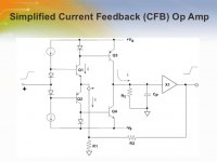
It is difficult to have a sensible technical discussion with someone who has private meanings for words. So when you say that the CFP is an opamp, all you meant to say was that the CFP includes local feedback - which is obvious and hardly needs saying.
😱 You have a private meanings, its exactly a power op-amp.
Its an op-amp with output connected to its -in (the emitter of the driver) without a divider because voltage gain is not needed in the case. One transistor can be driven from its base or from its emitter which is called common base.
Imagine a NPN transistor with resistors at its collector and emitter.
Feed a signal to its base and the result at the collector will be inverted.
Feed a signal to its emitter and the result at the same place will be the same, not-inverted.
This means that this configuration has two inputs: +in and -in
but need to be further inverted one more time to have the +in at its base
and the minus one at its emitter.
Now bias it to have 0V at its emitter, attach a VAS stage to it and you have a 2-3 transistor configuration that has +in, -in, voltage and current gain.
Its an op-amp if it has +in and -in and a VAS. NFB is nothing more than feeding the emitter's input from the output with or without a divider. LTP works the same but it has a current gain stage for the feedback because common base's input has a low Z. And exactly this is the most important => you need to have a divider with a very low R values to provide much current.
It won't work with high Z divider. In CFP the output its tied directly to the -in => the output can drive this input perfect.
This CG stage that LTP have is only needed in low power applications when there is not enough power for the feedback. For example: an oscillator circuit.
In audio power amplifier you have very much power and its better to have a low Z divider than a current gain stage.
Look at the attachment, Q1 and Q3 form a CFP when you connect the -in to the output.
Everything else is the same as a CFP output stage.
Attachments
Last edited:
Svitjod, its the common sense.
You know its good when its beautyful and feels good.
Linearity is not that important as the slew rate is and you can't have a high SR without a NFB. If you want a little distortion you can feed a NFB circuit with an EF stage outside the loop.
You like simplicity? Look at my 3 transistor op-amp circuit:
http://www.diyaudio.com/forums/solid-state/305696-single-transistor-op-amp-circuit.html
Personally, I like both distorted sound and clean but when I have to choose, I choose the clean one.
I will build an amplifier with a potentiometer for adjusting between distorted and clean sound to can adjust it when I want to.
Last edited:
I didn't understand what you are talking, write more understandable.
I am saying there are transistor .models that are questionable - some contributors to this forum have found it necessary to devise their own versions - notably Bob Cordell. Try substituting some of from his selection for transistor equivalents in your experimental circuit.
I suggest also before developing this further to try your circuit with increased supply rails in line with some reasonable power output - I take this is your ultimate purpose.
If you do this you will find the collector voltages for transistors with a load in series with that terminal will change and with that change in Miller capacitances - such being an inverse function of applied collector voltage.
There will be some changes too in transistor operating points to consider.
In the end you will have to build the circuit to see how close it is to the predictions of your simulations.
Have you listened to any of your simulations? This is possible apparently but I have no idea how and it probably devalues the accuracy of simulations even further
Yes but not yet the latest designs and also the currents was very close to the simulated ones. I haven't measured THD because I dont have such an analyzer.
I downloaded some software programs for this that can read from the Line In of the PC via a divider but I haven't tried yet.
mjona, now I understand you.
I know that but this is no problem for me since I use only famous, standart parts (BC546-549/556.., BC550/56..).
I believe they have proper models.
From my experience, there is a small difference between the real and the simulated but it can be avoided If you think how to trick it.
Otherwise, you dont have another option and have to adjust every circuit with a trimmer.
Its not a problem but its better to dont have to adjust.
You dont need to match all the characteristics, especially in feedback circuits.
I think the offset shows how good is a circuit.
My latest design have 2mV offset without the 220u which disconnects the feedback from ground. Im shunting this cap with a 10-15 ohm resistor because I think its better.
The important is to have the same currents and the offset will be the same as in the simulation. The trick to have the same currents is to use high value emitter degenerators.
You can simulate two different transistors in EF configuration with a very high load resistors and their currents will be the same with a same bias.
The only problem is the VAS stage where you can't use high value R.
You can program a AVR/PIC microcontroller to measure transistor's differences, collects them and show how close is a Q to the average. Or it can calculate how to change your circuit to use the Q for VAS.
I believe that If your circuit has a very low offset - its biased, ready to go and operating like it performs in the simulation.
In LTP circuits, the LTP transistors must be matched only when its current-mirror loaded and this is the only case that needs matched transistors.
Last edited:
No. A CFP output stage is not an opamp. See post 72 if you would like to know what an opamp actually is.darkshy said:You have a private meanings, its exactly a power op-amp.
No. See post 72. One of the features of an opamp is a significant degree of common-mode rejection.Its an op-amp if it has +in and -in and a VAS.
No, linearity is more important than slew rate - unless slew rate is dire. You can have high slew rate without feedback.Linearity is not that important as the slew rate is and you can't have a high SR without a NFB.
Have you listened to any of your simulations? This is possible apparently but I have no idea how and it probably devalues the accuracy of simulations even further
A couple of these are hardware I had already built which work adequately. Others are odd ideas I am looking into. They worked no problem using Modpex transistor .models however using Cordell ones led to changes in component values and transistor types.
I working on a board layout for a first attempt to build out of casual interest -more of test of SPICE simulation on something odd in a design.
No. A CFP output stage is not an opamp. See post 72 if you would like to know what an opamp actually is.
...
<~3-4 active devices typically don't have all of the desired properties to be called "op amps"
When you dont know that they can be one and bias them different.
The first transistor must be biased to have 0V at its emitter to be an input inverter stage for it and also I have another prove -> LTP is nothing more than this with an EF that only current gains the the feedback. It goes to the same place, are you stupid ?! The only difference is the EF stage between the emitter and the divider !!!!!
> "No, linearity is more important than slew rate - unless slew rate is dire. You can have high slew rate without feedback."
You can't have high SR without a feedback. Feedback forces it to rise/fall fast because gives more voltage when the output is on its way to the target.
You can, but cant have higher than a circuit with NFB and this means that you'll always have a good linearity too.
Thats why SR is more important, because you get a package if you go this way, you get both Linearity & SR.
If you go the other way you'll get the high Lin with less SR.
Linearity is important == SR's importance BUT you have to choose and I prefer the SR's way. Its paradoxical as everything it is.
mjona, I have an idea to build a PCB with connectors that will allow me to change things easily without the need of soldering.
This will help me to try different combos.
I know what is the best one but I want to try some.
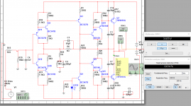
The best one I like is the attached one, my latest.
Its CFB + class A, CCS loaded VAS instead the standart push-pull VAS version.
First stages are class A, you have only push-pull out and drivers.
Very strong bonus is that the outputs are driven with EFs and its not darlington out.
The output stage is another CFB amp but with push-pull VAS stage (the output Qs)
Its not finished, I will make the input filter 2nd, 3rd order, I will make the VAS a compound to feed the capacitance better, I will filtrate the supply rails of the IPS with LPF RC networks...
BTW, I tried CCS shunted with a resistor for a VAS load and the result is better.
Half the current thry the CCS, half the current thru the resistor.
Maybe the best is CCS+resistor+bootstrap combo
You can make your own current ratio ;d
Im wondering about a phase splitter class A driver stage which drives two NPN outputs.
This will help me to try different combos.
I know what is the best one but I want to try some.
The best one I like is the attached one, my latest.
Its CFB + class A, CCS loaded VAS instead the standart push-pull VAS version.
First stages are class A, you have only push-pull out and drivers.
Very strong bonus is that the outputs are driven with EFs and its not darlington out.
The output stage is another CFB amp but with push-pull VAS stage (the output Qs)
Its not finished, I will make the input filter 2nd, 3rd order, I will make the VAS a compound to feed the capacitance better, I will filtrate the supply rails of the IPS with LPF RC networks...
BTW, I tried CCS shunted with a resistor for a VAS load and the result is better.
Half the current thry the CCS, half the current thru the resistor.
Maybe the best is CCS+resistor+bootstrap combo
You can make your own current ratio ;d
Im wondering about a phase splitter class A driver stage which drives two NPN outputs.
Attachments
Last edited:
You certainly seem to be keen to win the prize for dogged persistence in the face of facts.darkshy said:When you dont know that they can be one and bias them different.
The first transistor must be biased to have 0V at its emitter to be an input inverter stage for it and also I have another prove -> LTP is nothing more than this with an EF that only current gains the the feedback.
No. Jcx is not stupid either. The Mods may wish to feel your collar for using unparliamentary language to describe people who are trying (but, sadly, failing) to enlighten you.It goes to the same place, are you stupid ?!
I didn't understand what you are talking, write more understandable.
Ironic
Folk's, don't quibble too much about OP amps! For me, an OP amp is a black little bit of plastic with eight legs.
Darkshy, why do you mean that SR is important?
You don't really need more than a couple of V/us to deliver full voltage swing at audio frequencies.
Darkshy, why do you mean that SR is important?
You don't really need more than a couple of V/us to deliver full voltage swing at audio frequencies.
Folk's, don't quibble too much about OP amps!
many audio PA topologies are "op amps" - and many useful amplifier techniques and explanations are found in op amp technical literature
and a very good history of op amps is free: http://www.analog.com/media/en/training-seminars/design-handbooks/Op-Amp-Applications/SectionH.pdf
an annoying fight with audio design "gurus" is their all too common ignorance of EE history outside of their personal take on "audio" circuit design
this leads to them claiming inventions, insights that those aware of the broader history can show decades of priority for
this dynamic was very obvious in the AES Journal from ~ mid 1970's when SS audio power amp design issues enjoyed a relative surge of articles over a decade or so
Im wondering about a phase splitter class A driver stage which drives two NPN outputs.
That is what I have investigated. I am happy to share details with you if you are interested in seeing the .asc files. I have kept the rest of the circuit simple to see if it works. Seemingly it depends a lot on the choice of transistors - I chose MJL21194 for outputs the only other types that looked likely were 2N3716 a relatively high current gain type.
On the other hand, everything with audio amplification is probably invented by now. So what a guru does is to cook together a useful soup that he and his followers think sounds nice. But if he claims clever inventions he is probably "out bicycling" as we say in Sweden.
For some fifteen years ago, before I used to construct audio ( I didn't have the confidence ) I actually "invented" a fabulous little thing. I said to myself: "It's not every day one is creative - but the damn thing is probably patented already". And of course it was.
But they say no snowflakes are exactly the same. So there are probably very well sounding things "un-constructed". But you can't get a patent for it.
I recently "invented" a class AB BJT amplifier that only has two stages( within the NFB loop ) and still measures good. I'm very fond of it and I think it sounds great, but I can't get any patent for it.
Attempting to re-invent the wheel is, to my mind, a waste of time. It's usually in order to come up with something "new" to sell, so since this is how the world works it is necessary, but of course there is nothing new under the sun. In reality it's an effort to improve, and that can only be a good thing. Also it gives people something to do.
Attempting to re-invent the wheel is, to my mind, a waste of time. It's usually in order to come up with something "new" to sell, so since this is how the world works it is necessary, but of course there is nothing new under the sun. In reality it's an effort to improve, and that can only be a good thing. Also it gives people something to do.
I am not interested in selling anything just satisfying an idle curiosity. All NPN output stages are not uncommon in IC op.amps such as MC33078 and OPA 2604 .The reason for that is PNP is something to avoid if possiblei in fabricating audio types.
I am not expecting any special result as the idea of upscaling the circuit has not caught on and there will be reasons for that no doubt - the fact that with discrete transisors there is no need with a range of well researched topologies already extant.
I have been down that route but have not looked to see what there is that is odd for a change.
You certainly seem to be keen to win the prize for dogged persistence in the face of facts.
Thats you that .."dogged persistence in the face of facts."
I gave u 10000 proofs: almost simpliest op-amp is the CFB one which's schematic is the same as a CFP OPS schematic. WHERE YOU SAW THE DIFFERENCE ? SHOW ME ! I dont want to explain this 10000 times.
Im explaining only because this is very good to know and want to share it.
THERE CANNOT BE A DIFFERENCE WHEN THEIR SCHEMATICS ARE 100% == EQUAL SAME. Biasing the same, everything.. Maybe the diamond buffer biasing in some schematics makes you think they are different or what ?
Just prove it to me, you didn't proved, I proved.
Also I prooved with the LTP topology too which is the same but have a current amplifier for the feedback which doesn't make it different.
No. Jcx is not stupid either. The Mods may wish to feel your collar for using unparliamentary language to describe people who are trying (but, sadly, failing) to enlighten you.
Its obvious that I was talking to you, not jcx, and its obvious like the proofs
I gave u.
You knew that and lied to make it look like i use "unparliamentary" language.
No, I really didn't understanded. Maybe he edited his post and Its understandable now.Ironic
Folk's, don't quibble too much about OP amps! For me, an OP amp is a black little bit of plastic with eight legs.
Darkshy, why do you mean that SR is important?
You don't really need more than a couple of V/us to deliver full voltage swing at audio frequencies.
Because:
1. I prooved myself that the higher SR can drive a low biased output stage as it does with the high bias one. equal == THDs at 1 and 20khz
(I prooved in the simulator but it will be the same in reality too.)
2. Its possible to need more than the need (Dont know)
3. I felt it with my common sense
4. I don't know, I felt it and believe my 6th sense.
OK, Lets discuss it:
First of all, I believe some people didnt know that CFB's wants a low Z divider to give its better results, tried, saw the bad results and then a myth started to flying around..
Also many dont know how to bias properly CFB and VFB.
For the VFB:
1. Using current-mirror gives good results but makes the circuits very unreliable.
2. Everybody bias it to have an equal currents in the both collectors.
This is correct but only when you need the both LTP outs symmetric.
Its better to have the more tail current thru the FB's EF stage when you have a CCS loaded VAS because it feeds the fb more well and you lose nothing, you lose the 2nd phase out which you dont use in the case.
Try it and you will see the significant difference in the performance.
Im saying again that the simulated analyses may not be the same but they will be close enough and also I believe they will be the same if your offset is the same as in the simulation. The transistors are different and exactly this is the reason to use a FB circuit (u forgot why u are using a fb?). Also you can use a trimmer to adjust the offset.
And the one #3 -> LTP also performs better with a low Z fb divider and it must as lowest as possible.
For the CFB's bias:
I believe people dont know there must be 0V at the emitters.
/!\
---------------------------------------------------------
IM GOING TO SAY SMTH REALLY IMPORTANT HERE
!!! READ !!!!
{
I thinked that the higher SR can fix the crossover distortion issue with less bias -> a veeery less bias: 200pA for example and that way we can build the circuits without a Vbe multiplier and have no thermal runaway problems.
Then simulated a CFB to see if my theory is true (but not a standart one with a push-pull VAS, i tried it CCS load like its a VFB),
and guess what: I was totally amazed because it worked. It gave me such a low THD @ 20k and 200pA bias that I've never seen before with 200pA OPS bias and VFB.
I have simulated many VFB circuits and never seen this, its exactly the way I like it -> I prefer to not have a Vbe multiplier (I like VbeM very but prefer it without it)
It seems that the SR's difference is not so small.
}
----------------------------------------------------------
ANOTHER IMPORTANT HERE: /!\
{
As I mentioned: both CFB and VFB are almost the same with the only difference that VFB has one more stage for providing more current because of the -in's impedance of the CFB which is low. This current you need, only when you need it and in the case of the audio amplifier, you have even more that looks infinite when compared to the -in's wantage/needs.
Whats the point to have an extra transistor when you can provide the current with two power resistors for a divider.
There is no point: you only lose a transistor, add capacitance and lose speed.
Linearity must be the same because both CFB and VFB are cool.
I think CFB's little better but lets assume they have a same one.
Lets assume that half of us prefer to lose transistor and the other half prefer to save it. This one is from the paradoxical ones so it belongs to "We all have equal rights -> the both tastes true"
And lets summary:
Linearity - same
Losing transistor - same
SR - CFB wins because of the VFB's EF stage itself and its capacitance.
Capacitance - CFB wins
Summary of the summary:
CFB wins for the applications that can afford its current need even if you think that u dont need the extra SR because you're losing nothing and saving a transistor.
Summary of my belief:
I think that its better to have a higher SR than you need because it can drive a low biased ouput stage (200pA) with the same THDs as it does with a 100mA bias.
}
- Status
- Not open for further replies.
- Home
- Amplifiers
- Solid State
- Question about class B output stages