Hello, after a long time, I've finally built a working amp based on the designs discussed on THIS thread.
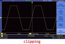
What I can say right away is: I was impressed with how the circuit showed great stability on a breadboard and with no compensation network, no thermal feedback and exhibited symmetrical clipping and no visible crossover distortion even at insufficient bias.
The circuit (all components used are exactly the same):

Shown below is the early prototype (with much reduced parts count):

Final prototype (25000uF per rail):

Now let's jump to the measurements:
Some extra considerations:
— Sound card used was a Creative Sound Blaster X-fi HD (SB1240);
— You can get more than double the SR by changing the compensation network and the low pass input RC filter, I only chose these values so I could show that the amp is stable with unrealistic capacitive loads;
— I only chose a TL081C as DC servo because I didn't want to use my expensive JFET input op amps (also it'd be a pain to solder because they're all SMD) but I encourage everyone to use something better, the datasheet says it's immune to latch-up but THAT'S A LIE, and a HUGE problem if your finished design doesn't have output DC protection;
— I couldn't realiably measure damping factor at and above 10kHz because my multimeter does not have the bandwidth (I don't think most of the do anyway) and my scope doesn't have the accuracy (I was measuring at full power output) for measuring high voltages with mV precision, but I have strong evidence that the DF doesn't stray far from the 1800:1 across the entire audio spectrum;
— I didn't measure IMD at full power because the generator was the same external sound card that was analyzing the output signal and I had no way to isolate the input to prevent a ground loop (at low power it was fine because no high currents were involved and the grounding layout worked fine). For those interested, it measured 0.045%;
— The heatsink used is working on its limit, I had to set the idle (cold) current very high to achieve the idle (hot) current I wanted. Before I realized this, the insufficient heatsink size made it so that after 30min the idle current had fallen way below what I had set initially. I recommend choosing a bigger heatsink;
— You can extract more power from the circuit by making the driver stage a single BJT emitter follower instead of the discrete Darlington emitter follower I chose, at the cost of higher loading of the VAS;
— The amp was not tested with 4R loads because my transformer can't supply enough current, thought the circuit can probably handle 4R without problems.
Applying capacitive loads:
I will not be supplying the .asc file (unless someone really wants) because I don't have most of the models, I just renamed the components on the schematic above to match what I used in real life.
What I can say right away is: I was impressed with how the circuit showed great stability on a breadboard and with no compensation network, no thermal feedback and exhibited symmetrical clipping and no visible crossover distortion even at insufficient bias.
The circuit (all components used are exactly the same):
Shown below is the early prototype (with much reduced parts count):
Final prototype (25000uF per rail):
With only one pair, the THD was limited to 0.005% @1W and 0.030% @50W, adding an extra pair allowed me to have much better THD at full power and also increased the Damping Factor from ~300 to the values shown below.I see you doubled the output devices for only 50W output, why was that?
Now let's jump to the measurements:
- Frequency Response: 4Hz ~ 147kHz
- Noise (Max Vpp): <20mVpp
- Noise (Max Vrms): <4mVrms
- Slew Rate: >30V/us
- Max DC Offset: <3mV
- Damping Factor (50W/8R/20Hz): 1820
- Damping Factor (50W/8R/100Hz): 1870
- Damping Factor (50W/8R/1kHz): 1870
- THD (1W/8R/1kHz): <0.002% (limited by signal gen. THD)
- THD (50W/8R/1kHz): <0.006%
- Phase Shift @20kHz: <10.2°
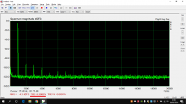
- IMD (1W/10kHz+11kHz/1:1 ratio): <0.004%
- Input Sensitivity: 360mVrms
- Voltage Gain: 34dB
Some extra considerations:
— Sound card used was a Creative Sound Blaster X-fi HD (SB1240);
— You can get more than double the SR by changing the compensation network and the low pass input RC filter, I only chose these values so I could show that the amp is stable with unrealistic capacitive loads;
— I only chose a TL081C as DC servo because I didn't want to use my expensive JFET input op amps (also it'd be a pain to solder because they're all SMD) but I encourage everyone to use something better, the datasheet says it's immune to latch-up but THAT'S A LIE, and a HUGE problem if your finished design doesn't have output DC protection;
— I couldn't realiably measure damping factor at and above 10kHz because my multimeter does not have the bandwidth (I don't think most of the do anyway) and my scope doesn't have the accuracy (I was measuring at full power output) for measuring high voltages with mV precision, but I have strong evidence that the DF doesn't stray far from the 1800:1 across the entire audio spectrum;
— I didn't measure IMD at full power because the generator was the same external sound card that was analyzing the output signal and I had no way to isolate the input to prevent a ground loop (at low power it was fine because no high currents were involved and the grounding layout worked fine). For those interested, it measured 0.045%;
— The heatsink used is working on its limit, I had to set the idle (cold) current very high to achieve the idle (hot) current I wanted. Before I realized this, the insufficient heatsink size made it so that after 30min the idle current had fallen way below what I had set initially. I recommend choosing a bigger heatsink;
— You can extract more power from the circuit by making the driver stage a single BJT emitter follower instead of the discrete Darlington emitter follower I chose, at the cost of higher loading of the VAS;
— The amp was not tested with 4R loads because my transformer can't supply enough current, thought the circuit can probably handle 4R without problems.
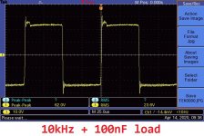
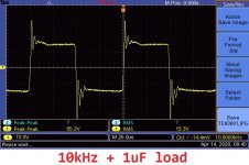
Applying capacitive loads:
- 1nF and lower: no visible change
- 10nF: no visible change
- 100nF: small oscillation over the negative part of the square wave
- 1uF: very large overshoot but stops immediately, doesn't break down into a chaotic oscillation
I will not be supplying the .asc file (unless someone really wants) because I don't have most of the models, I just renamed the components on the schematic above to match what I used in real life.
Attachments
-
 1kHz sqr.jpg111.2 KB · Views: 547
 -
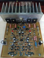 IMG_1.jpg637.6 KB · Views: 176
 -
 clipping.jpg112.1 KB · Views: 148
 -
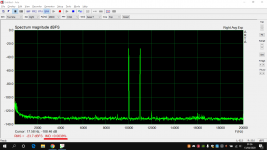 IMD 10-11kHz 1W.png48 KB · Views: 127
 -
 THD 50W.png48.9 KB · Views: 126
 -
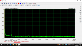 THD 1W.png48.1 KB · Views: 129
 -
 1000nF load.jpg104.4 KB · Views: 133
 -
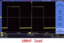 100nF load.jpg109.2 KB · Views: 127
 -
 20kHz sqr.jpg115.1 KB · Views: 134
 -
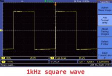
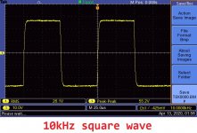 10kHz sqr.jpg116.1 KB · Views: 560
Last edited:
Hi BF245C, one quick question on your circuit. What sets the current on Q22 and Q19, the VAS transistors, in your circuit?
Nice results btw.
Best, Sandro
Nice results btw.
Best, Sandro
Hi Sandro, thanks for replying.
What sets the VAS current is the voltage drop across R16 and R17, these resistors are also the emitter degeneration resistors of the current mirror formed by Q20/Q28 and Q21/Q29.
What sets the current on the whole current mirror is the sink-source CS made by Q14 and Q25. This CS is set to ~1mA so the emitter resistors have a drop of ~1V (which is enough degeneration for a current mirror and a reasonable voltage for setting the VAS current).
This current mirror acts as both a way to set the VAS current (the primary goal of this project) and as a beta-enhance emitter follower to lighten the load seen by the IPS.
The reason I asked is because this push-pull VAS, which has been discussed to no end, has undetermined bias current on Q22 and Q19.
I thought your circuit addressed this issue somehow, but I don't see it. What am I missing?
Thanks for sharing!
Best, Sandro
I thought your circuit addressed this issue somehow, but I don't see it. What am I missing?
Thanks for sharing!
Best, Sandro
Last edited:
I see it now. Q29 and Q20 are diode connected. Interesting!!!
Essentially you have formed a current mirror between Q29-Q21 and Q20-Q28.
Do you have an .asc for this. I would love to play with this design.
Thanks in advance!
Essentially you have formed a current mirror between Q29-Q21 and Q20-Q28.
Do you have an .asc for this. I would love to play with this design.
Thanks in advance!
Last edited:
I see it now. Q29 and Q20 are diode connected. Interesting!!!
That's right, maybe it was difficult to see because I also shared that node with the feedback network, my bad.
I'm sending the .asc, also note that:
* All the 2SA/2SC except the 5200s/1943s don't have a model but can be swapped for the BD139/140 (which I included the models)
* None of the zeners have a model but can be swapped for equivalent Vz ones from the LTSpice library
* The bias current for the output stage will be all over the place because these are the values I used for real life parts
* If you think you have better models for the transistors, please use them, I wouldn't put my hand on fire for these models
* If it oscillates, try using normal miller compensation instead of this transitional miller compensation
* The cascode LED model for the VAS doesn't work, use a 1.8V zener instead or 3x1N4148
* The TL081C doesn't have a model, I actually used an AD823A during simulations
Have fun!
Attachments
I count 45 transistors in total (ex U1).
Are Q8 and Q10 doing fine? I'd prefer some more robust types here, especially when switching on.
There's not so much rail-regulation however. Regulation is done on various other places, but that's a trade off.
Input impedance is only 5kΩ, a bit low?
Are Q8 and Q10 doing fine? I'd prefer some more robust types here, especially when switching on.
There's not so much rail-regulation however. Regulation is done on various other places, but that's a trade off.
Input impedance is only 5kΩ, a bit low?
Are Q8 and Q10 doing fine? I'd prefer some more robust types here, especially when switching on.
Unbelievably, yes, they don't heat up at all (I don't think they dissipate even close to 50mW), since they only handle the currents from before the driver stage.
During the tests I've tried TIP41C/42C and BDX53C/54C (darlingtons) and ended up choosing the little guys because they had more gain than the TIPs and dropped less voltage across than the BDXs. Didn't think about turn-on currents though, that may indeed be a problem, the datasheet for the BC546 doesn't even list peak current capabilities.
There's not so much rail-regulation however. Regulation is done on various other places, but that's a trade off.
Unfortunately I don't have the waveforms saved but I checked that too and the difference between the dirty output stage rails and the voltage supplied to the small signal stage is bigger that you would think. I don't think I'll ever design another amp without capacitive multipliers.
Input impedance is only 5kΩ, a bit low?
You're right, it only works with a 10k input resistor because the input cap is a 4.7uF MLCC (insane capacitance for the size). I wouldn't use ceramics on the signal path of a final version though.
If I ever get the courage to design a proper PCB, the high pass RC filter will be a 3.3uF Epcos MKT with a 47k resistor, and the input parallel resistor (R83) will be more close to 100k, giving close to 32k input impedance.
Last edited:
Did you notice bass enhancement with 2 pairs of outputs?
To be fair I haven't listened the finished version at a high volume yet, the lockdown makes everything seem more quiet.
The biggest enhancement in bass during the project was when I changed the reservoir caps from 5000uF to 25000uF 😀
Attached: 100mA, but the beta-rolloff starts from 40mA....the datasheet for the BC546 doesn't even list peak current capabilities...
That will be the main supply value minus Vbe Q8/Q10: +/-36.3V....and the voltage supplied to the small signal stage is bigger that you would think...
Attachments
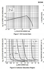

Attached: 100mA, but the beta-rolloff starts from 40mA.
Oops, I meant "pulsed collector current". About the beta rolloff I think I got lucky, the max current I'm passing through them is 35mA.
That will be the main supply value minus Vbe Q8/Q10: +/-36.3V.
Sorry, I meant to say the difference in the levels of ripple haha. In my defense, I should already be sleeping.
C46 worries me - it seems to directly couple differential-mode rail noise into the signal path, or put another way the constant current section has severely limited bandwidth.
I would be interested if you have any PSRR measurements for either rail?
One of the things I do with emulated amp circuits is to put a 1V rms ripple signal onto each rail at different frequencies to see how much leaks into the output, this helps chase down bad placements of decoupling caps - some signals are referenced to ground, some to a rail, its important to decouple to the right place for good PSRR.
The damping factor can be measured emulated or real life by putting a voltage signal inline with the load, thus injecting a current into the amp's output, measure the voltage this creates, gives output impedance.
That's the same (to me): Pd=625mW, so given a max Ic of 100mAdc and with a Vbe of 0.625Vdc you're already there. There is hardly some pulsed margin, or deliberately not specified. I've not calculated the current demand from the front stages yet, but above say 40mA things might become a bit more risky due to the beta drop.Oops, I meant "pulsed collector current".
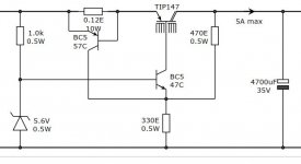
Ripple rejection is also depending on the load; I'd still prefer another configuraion. If you want a low drop to keep the front on high enough voltages, better use a regular low drop regulater. It consists basically of two transistors, three resistors, a zener and a cap. It's a high loopgain regulator as applied in commercial supply regulators. I've added an example of the 12V version with current protection for my motorcycle. Adapt the various values to your needs.
Attachments
Indeed so. Intended to have both separated signals from the input differentials to become the same again (if the differentials have a little but significant gain difference - should the feedback take care off), so this is a [adjective] drawback of such a topology.C46 worries me - it seems to directly couple differential-mode rail noise into the signal path, or put another way the constant current section has severely limited bandwidth.
I think you have shown capacitive loading at 1kHz. Try now 10 kHz...😉
You seem to have a gain of about 50 so with +/-37vdc PSU you will have to get low input voltage for max output.I suppose that it is for system without preamplifier gain and low amplitude signal source such as a phono preamplifier stage?
You have fuses for output stage protection but do you have protection for the front stage...
Fab
Last edited:
exhibited symmetrical clipping and no visible crossover distortion even at insufficient bias.
Is this with a speaker load connected?
It's an interesting design. I do prefer my 12-transistor < 0.01% THD designs for their simplicity (and yes, I've designed far more complex designs), but your results look impressive. I don't enjoy using current mirrors much, but in this design they're probably better because it looks like their current is really low.
This makes me want to break out my symmetrical design I once prototyped. I think I abandoned the design just because I found the complexity unnecessary. I suppose if I had to sell amplifiers, the better specs would make nicer marketing.
C46 worries me - it seems to directly couple differential-mode rail noise into the signal path, or put another way the constant current section has severely limited bandwidth.
I would be interested if you have any PSRR measurements for either rail?
It makes sense, at high frequencies C46 acts like a low resistance in parallel with the ideally infinite resistance of the CS.
Just tried measuring the PSRR and I couldn't obtain any results with my gear. I tried injecting a signal from my signal gen. into the rail via a 220uF non-polarized electrolytic but the impedance shown by the power rails is so much lower than the signal gen. output impedance that the signal doesn't even appear.
So I tried injecting the 1kHz signal at the clean rail (after the capacitive multiplier), kind of worked but the injected wave had clean crests and flat troughs. a low amplitude would not produce anything measurable on the output and a high amplitude would produce glitches on the output (which I determined to NOT be the signal I was injecting because it was exactly 180° out of phase, didn't grow linearly with the increases on the injected signal and was around 10x smaller than the signal injected, as bad as this amp may be, I doubt it has only 20dB PSRR).
Then I searched for and old LTSpice simulation of this circuit that works and tried measuring PSRR. Just like I saw in practice, injecting 1Vrms of noise into the positive rail was too much and produced similar glitches to those I had just saw. So I tried measuring the PSRR anyway, results: 67dB.
Then I reduced the noise amplitude to 0.3Vrms, the glitches were gone and I could measure the output, results: 90dB PSRR.
I don't think I'll be trying to measure any power amp PSRR again until I build a power supply where I can directly modulate the output.
That's the same (to me): Pd=625mW, so given a max Ic of 100mAdc and with a Vbe of 0.625Vdc you're already there. There is hardly some pulsed margin, or deliberately not specified. I've not calculated the current demand from the front stages yet, but above say 40mA things might become a bit more risky due to the beta drop.
Well, I guess there's no escaping from Darlington/Sziklai configurations then. Also, there is indeed no regulation per se but there is a lot of ripple rejection being done by the capacitive multiplier, I've attached below the waveforms of the power rail vs the clean rail.
If you want a low drop to keep the front on high enough voltages, better use a regular low drop regulater.
Yes, for my next project (not a power amp though) I'll be using the low-noise high-PSRR LDOs I have in hand (NCP565).
I don't know if the following reasons are valid but what made me choose capacitive multipliers here was:
* Their output voltage is always the highest possible;
* Didn't have LDOs that support 37V rails;
* I'm on the end of the power line so mains voltage varies a lot, I didn't want to run the risk of the rectified voltage falling below the LDO threshold for a given output voltage.
I think you have shown capacitive loading at 1kHz. Try now 10 kHz...😉
Tried, no changes to 10nF and below, minor changes to 100nF and 1uF still didn't send the amp into total oscillation. Pictures for 100nF and 1uF are attached below.
You seem to have a gain of about 50 so with +/-37vdc PSU you will have to get low input voltage for max output.I suppose that it is for system without preamplifier gain and low amplitude signal source such as a phono preamplifier stage?
Not really, most consumer electronics today have very good THD performance at low volume levels and yet become utter trash at higher volume levels, so I'll pretend that I designed it to have more headroom.
What really happened was that my crappy signal gen thinks that Amplitude = Vpp instead of Vp, so when I finally realized it, I had already designed the amp with too much gain.
You have fuses for output stage protection but do you have protection for the front stage...
Nothing for the front stage. I thought of adding two transistors to sense overcurrent on the VAS via R15/R18 but I have no practice with VI limiters so I chose not to.
Is this with a speaker load connected?
Yes, I even remember having the 8R load connected, looking at the spectrum analyzer and seeing no significant THD increase even when I cranked the bias to zero, then I checked on the scope later and saw no crossover point.
This makes me want to break out my symmetrical design I once prototyped. I think I abandoned the design just because I found the complexity unnecessary. I suppose if I had to sell amplifiers, the better specs would make nicer marketing.
Only if the marketing is able to compensate for the extra parts cost, haha.
Attachments

Last edited:
...I don't think I'll ever design another amp without capacitive multipliers...
...after the capacitive multiplier...there is a lot of ripple rejection being done by the capacitive multiplier...what made me choose capacitive multipliers here was...
I think I'm misinterpreting and thus not understanding your phrases about this completely. Apart from given motivations, can you highlight these capacitive multipliers in the design?
I think I'm misinterpreting and thus not understanding your phrases about this completely. Apart from given motivations, can you highlight these capacitive multipliers in the design?
I'm sure it's C40 and C41.
- Home
- Amplifiers
- Solid State
- Push-Pull VAS [50W@8R]