Hey all,
I have a Punch x360.2 on the bench, board # PC-3081-C. I am wondering if anyone can help me obtain the schematic?
Owner hooked it up backwards and fried the power supply FET's. I replaced them with the closest equivilant I could find (IRLZ44PBF). Beeped out the rest of the board and couldn't find any other bad components. It powers up now but the rail voltage isn't stable and there's excessive current draw.
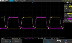
Is anyone familiar with the switching wave forms on these era of amps (both gate and drain)? I'm seeing a bit of crossover on the transitions and wondering if the issue is the devices I chose.
I attached the gate and drain wave forms.
Thank you!
I have a Punch x360.2 on the bench, board # PC-3081-C. I am wondering if anyone can help me obtain the schematic?
Owner hooked it up backwards and fried the power supply FET's. I replaced them with the closest equivilant I could find (IRLZ44PBF). Beeped out the rest of the board and couldn't find any other bad components. It powers up now but the rail voltage isn't stable and there's excessive current draw.
Is anyone familiar with the switching wave forms on these era of amps (both gate and drain)? I'm seeing a bit of crossover on the transitions and wondering if the issue is the devices I chose.
I attached the gate and drain wave forms.
Thank you!
Attachments
Last edited:
Those are logic level FETs and may not be suitable for the drivers as they are now. You could try installing a 470 ohm resistor across the collector and the emitter of each of the two PNP driver transistors. If that reduces the heating, the logic level FETs are likely the problem.
Attachments
Thanks for the reply. If it helps, the original FET's were 50N06V, which is what I attempted to cross reference. Not BUZ11 as shown on the schematic. Also, D10-D13 do not look to be present.
It appears the supply is running at 100% pulse width, which seems odd but I'm not sure, let me know if this is normal.
It appears the supply is running at 100% pulse width, which seems odd but I'm not sure, let me know if this is normal.
Last edited:
What's the DC voltage on the B+ and remote terminals with the black probe on the ground terminal of the amp?
The amp will work normally (for testing) without those diodes. Do they look like someone removed them?
The amp will work normally (for testing) without those diodes. Do they look like someone removed them?
+/- 36.7v on the rails. 13.5v B+. D10-D13 were not removed, rather they do not appear anywhere on the board.
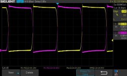
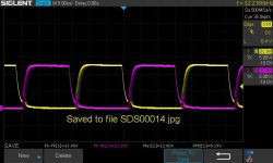
What's happening is a few seconds after turning on, the wave forms glitch about once per second while at the same time my 10A bench supply briefly hits current limit. It's hard to capture in a still but I was ablt to grab this one. This happens over and over until power is removed.
Using a FLIR I do not see any components getting unusually hot.
Attachments

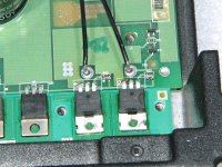
My bad, they are there exactly like you show. I mistook them for transistors with my eye sight failing. I have not yet, but I will try your suggestion.
Just the PNP drivers, Q1 and Q2. These will help pull the drive signal to ground.
If it still pulls excessive current, set the bias pots fully CCW.
If it still pulls excessive current, set the bias pots fully CCW.
Here are three captures. One before overcurrent, one during the transition into overcurrent, and lastly while in overcurrent. I'm starting to think my bonehead idea to put in IRL devices (with higher gate capacitance as well) is causing cross conduction.
Attachments

In some amps, the bias pots are backwards. If you let it try to power up repeatedly, are ANY of the output transistors heating up?
All of the transistors are heating up pretty evenly. I just ran a test 1khz signal through it, both channels are going on/off along with the overcurrent.. Like a 1khz busy signal. beep beep beep.
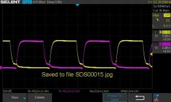
They are not heating up much. Stabilized power supply draw is 0,7 amps. Stabile duty cycle looks like the 1st capture of the three I posted last.
I need 3 voltages.
Black on pin 7 of the 494 IC. Red on pin 1?
Black on pin 7 of the 494 IC. Red on pin 2?
Red on pin 1, black on pin 2?
Black on pin 7 of the 494 IC. Red on pin 1?
Black on pin 7 of the 494 IC. Red on pin 2?
Red on pin 1, black on pin 2?
huge instability, overcurrent, and static noise from PS touching either pins one or 2, immediately I powered off before something bad happened each time.
- Home
- General Interest
- Car Audio
- Punch X360.2 schematic / advice