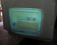
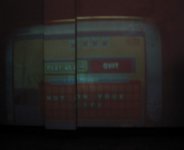
you would noticed a yellowish shade on the upper right and lower left corner of the screen. this is the edge of the fresnel and this i realized i cut the fresnel short and off center.
i tried to move the fresnel near the LCD and the this yellowish shade is eliminated but brightness is greatly reduced.
i tried to move the fresnel near the LCD and the this yellowish shade is eliminated but brightness is greatly reduced.
Attachments
what are your measurements from light-->mirror, mirror--> fresnel, fresnel-->lcd, and lcd-->lense.
also what do you think the fl on the fresnels are? i are interested to try my own pj of this sort
also what do you think the fl on the fresnels are? i are interested to try my own pj of this sort
ukagr said:what are your measurements from light-->mirror, mirror--> fresnel, fresnel-->lcd, and lcd-->lense.
also what do you think the fl on the fresnels are? i are interested to try my own pj of this sort
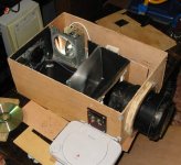
rough measurement was: light > mirror =4", mirror >fresnel = 4",
fresnel > LCD = 6", LCD > back lens of CRT Projection Lens = 0.5". or LCD > front lens of CRT projection lens = 6.5"
the unsplit fresnel would be aboout 12.5" distance from the front lens. i guess this is the typical FL of fresnel for OHP
this set up gives the brightess image, unfortunately i cut my fresnel short and off center. the fresnel was cut to 8" X 6" with center ring off by 1".
thanks for the info! How big have you got your image up to? Did you say you had a 75w mh bulb? Where did you get that from?
ukagr said:thanks for the info! How big have you got your image up to? Did you say you had a 75w mh bulb? Where did you get that from?
the diagonal image size is 1:1 of the throw distance. the last adjustment i did gave a decent brightness for a 2.5 meter diagonal.
i use an OSRAM brand 70watt MH. this type of bulb is commonly available on lamp/bulb hardware here in Manila.

Rmpmla, can you post the schematic of this mod please mate...
http://69.93.183.37/1797/26/upload/p4777242.jpg
Also, will it work on the official PSone screen??
http://69.93.183.37/1797/26/upload/p4777242.jpg
Also, will it work on the official PSone screen??
Gizmotech said:Rmpmla, can you post the schematic of this mod please mate...
http://69.93.183.37/1797/26/upload/p4777242.jpg
Also, will it work on the official PSone screen??
hi Gizmotech,
this is the link for the pin outs of the PSx game console.
http://www.gamesx.com/avpinouts/psxav.htm
this is the link for the VGA mod, you would see the schematics on post #126
http://www.mp3car.com/vbulletin/showthread.php?t=13313&page=9&pp=15
yes, this is the schematics use for Sony PSone screen.
it looks like pin 5 and 6 on the psx side is not connected to anything. can you shed some light on that area please.
Gizmotech said:it looks like pin 5 and 6 on the psx side is not connected to anything. can you shed some light on that area please.
yes, either of the pin 5 or 6 is connected as C- sync on the schematic coz there was a discussion on this as which of the pins is the real C-sync.
the C-sync was left open for connection ( between 5 and 6) and up for anyone to try by putting jumper wire.
based from the PSx pin out, pin 6 is the composite sync and this is what i have tried and it worked.
just an added info🙂 , you don't need this circuit if your video card has C-sync. not all video cards has this and i was able to check mine using Powerstrip.
So this is more like the correct PCB design for the official Sony PSone screen which has been tested and confirmed working by you??? Also that PCB design, Which side is the underside and which side is the components mounted on. I'm assuming the side that we are looking at is the side we solder on and the opposite side is where we mount the components?
Attachments
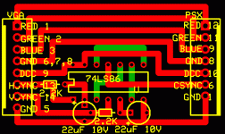
Gizmotech said:So C sync from the pcb design, you link/bridge it to either pin 5 or pin 6 on the psx side?
yes🙂 the foil path labelled c sync underneath pin 5 on the PSx side.
Gizmotech said:So this is more like the correct PCB design for the official Sony PSone screen which has been tested and confirmed working by you??? Also that PCB design, Which side is the underside and which side is the components mounted on. I'm assuming the side that we are looking at is the side we solder on and the opposite side is where we mount the components?
nice re-work on the schematics or there is already an updated one? for the test of PCB design, i came in quite late for this VGA mod and the guys from that forum are the ones that has tested it fully.
just got lucky it worked for me too🙂
the schematic as i interpret it ( anyone can correct me on this), is the component side.
hope to be of help Gizmotech
Thanks rmpmla. you've been a lot of help.
Yep, i've just studied the schematics and you were correct. Looking at the pic is the component side and the opposite side is the solder side. So the correct PCB design would have to be inverted before printing and mounting the components.
Yep, i've just studied the schematics and you were correct. Looking at the pic is the component side and the opposite side is the solder side. So the correct PCB design would have to be inverted before printing and mounting the components.
Here, this should help the confused like me. I hope you don't mind MatrixPC for editing your original design to make it easier for other people like me who has a little bit of difficulty to understand the design. Also many thanks to my pal Rmpmla for all his help.
Attachments

- Status
- Not open for further replies.
- Home
- General Interest
- Everything Else
- The Moving Image
- DIY Projectors
- psone LCD using CRT lens