MC34161 runs at HV, has two channels that can be set to opposite polarity to drive SDZ and MUTE, and costs about a buck. I'll probably figure out a way to use it here.
Yeah, i had them also on my mind. But in the end its just 2 comparators, so part count won't be less.
Yeah, gave up trying to make the 34161 work.
Got a 6 position DIP switch crammed in there allowing full master/slave gain selection. 3 switches connect resistors to GVDD (30.1K, 75K, 150K) and 3 switches connect the same 3 resistors to ground. How to use it:
20dB master: 30K to ground, rest open
26dB master: 30K to ground + 150K to GVDD
32dB master: 30K to ground + 75K to GVDD
36dB master: 30K to ground + 150K to GVDD + 75K to GVDD
20dB slave: 75K to ground + 75K to GVDD
26dB slave: 30K to GVDD + 75K to ground + 150K to ground
32dB slave: 30K to GVDD + 75K to ground
36dB slave: 30K to GVDD + 150K to ground.
This means you need a separate sheet of paper to know what switches to flip for a given setting, and you can probably end up with invalid settings pretty easily, but hey, it means no reworking of SMT to master/slave boards.
Pogo pin test points are added too. After seeing the pogo pin tester DUG's got built for his PBTL card, I've decided I'm doing the same thing, and testing a TPA3118 and nothing else is definitely feasible to do.
To do:
- finalize BOM, come up with prices for everything
- design pogo pin test PCB
- throw together a crappy website to host documentation/info on the card.
edit, latest snapshot:
I would have been happy with a couple of bridgeable solder pads for the gain settings. It will be interesting to see what the dip switches add BOM wise.
As for the stuffing options, If you are going to run this down an SMT line (rather than hand solder like DUG did) the NRE costs rare the same whether you place and reflow one part or all of them.
I think 3 kit options would meet most everyone's needs:
1) Bare
2) Full SMT
3) Full SMT with kitted through hole parts
Optionally: A fully turnkey board (ala cAMP) if you want to sell them on an ongoing basis.
Yeah, gave up trying to make the 34161 work.
Got a 6 position DIP switch crammed in there allowing full master/slave gain selection. 3 switches connect resistors to GVDD (30.1K, 75K, 150K) and 3 switches connect the same 3 resistors to ground. How to use it:
20dB master: 30K to ground, rest open
26dB master: 30K to ground + 150K to GVDD
32dB master: 30K to ground + 75K to GVDD
36dB master: 30K to ground + 150K to GVDD + 75K to GVDD
20dB slave: 75K to ground + 75K to GVDD
26dB slave: 30K to GVDD + 75K to ground + 150K to ground
32dB slave: 30K to GVDD + 75K to ground
36dB slave: 30K to GVDD + 150K to ground.
This means you need a separate sheet of paper to know what switches to flip for a given setting, and you can probably end up with invalid settings pretty easily, but hey, it means no reworking of SMT to master/slave boards.
Pogo pin test points are added too. After seeing the pogo pin tester DUG's got built for his PBTL card, I've decided I'm doing the same thing, and testing a TPA3118 and nothing else is definitely feasible to do.
To do:
- finalize BOM, come up with prices for everything
- design pogo pin test PCB
- throw together a crappy website to host documentation/info on the card.
edit, latest snapshot:
You have done a good layout without any remarks...

You no doubt already compared, but does the 1nF have positive contribution? Distance from chippin corrected for sim without 1nF?
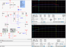
Yay decoupling simulation. Trying various parts and package sizes now to achieve a low wideband impedance.
An externally hosted image should be here but it was not working when we last tested it.
Black curve (unlabeled) is the ugly one. When capacitor #1 is above its series resonance and capacitor #2 is below, you effectively get a L and C in parallel which form a tuned circuit, creating a high impedance at their resonance. Ideally these don't end up anywhere where the amp will put a harmonic...
gmarsh, why not printing the gain table at the bottom silkscreen.
I finally would suggest to have a FAULTZ led driven by transistor. I actually using that pin as a current sink (3mA max, TI said), so having PVCC -> 10k -> Led -> FAULTZ. SDZ might get connected to FAULTZ with a jumper to have the self-clearing switchable.
I finally would suggest to have a FAULTZ led driven by transistor. I actually using that pin as a current sink (3mA max, TI said), so having PVCC -> 10k -> Led -> FAULTZ. SDZ might get connected to FAULTZ with a jumper to have the self-clearing switchable.
Last edited:
TDA3118 PCB
makes sense that this board needs differential analog inputs for decent S/N
I guess ideally a DAC interface with a volume control, but most don't have balanced outputs correct? so how can I use this amp. any recommendations?
I reckon most will use a laptop brick thingy , hoping some brand name ones might be better than a no-name one.
BTW the layout is looking great!
6 position SOIC switch versus 2 position adds about $1.50 CAD to the cost of the card. Not too worried about that, I can save double that figure by changing the terminal blocks from Phoenix rising cage ones to cheap screw ones.I would have been happy with a couple of bridgeable solder pads for the gain settings. It will be interesting to see what the dip switches add BOM wise.
As for the stuffing options, If you are going to run this down an SMT line (rather than hand solder like DUG did) the NRE costs rare the same whether you place and reflow one part or all of them.
I think 3 kit options would meet most everyone's needs:
1) Bare
2) Full SMT
3) Full SMT with kitted through hole parts
Optionally: A fully turnkey board (ala cAMP) if you want to sell them on an ongoing basis.
Here's the options I considered for the switch:
2 position (shown previously): 30.1K permanent to ground, 75/150K selectable to GVDD. Want slave mode, yank the 30.1K and install a resistor on a provided footprint.
3 position: 3rd switch disconnects 30.1K resistor, so you can leave it in place on the PCB, and add two of your own resistors on two provided footprints.
4 position: same as 3 position, 4th switch disconnects external resistor divider from GAIN/SLV so you can quickly switch between your own resistor pair or the built-in master options. Note that this may put extra loading on the TPA GVDD pin - they prefer you don't put anything over 100K resistive on GVDD, but then they put 60K on it on the evaluation board...
5 position: same as 4 position, 5th switch disconnects GVDD from external resistor divider to shed GVDD current draw.
6 position: "anything goes"
3 position is definitely better than 2 at making it easier to return to master mode, 4 position makes it really easy plus it's handy because there's already a 4 position switch on the card for AMx/MODSEL selection, 5 feels pointless compared to 6, and 6 means you don't have to solder anything for slave mode (well, other than the sync jumper to the next card over)
6 it is! It is clearly the most flexible option and not much more $
I was just thinking that all resistors could be populated and then the user could simply solder bridge the option they wanted. More work than switched and better than changing components.
I was just thinking that all resistors could be populated and then the user could simply solder bridge the option they wanted. More work than switched and better than changing components.
Once you've got the board bolted in place, bottom silkscreen isn't that useful.gmarsh, why not printing the gain table at the bottom silkscreen.
I finally would suggest to have a FAULTZ led driven by transistor. I actually using that pin as a current sink (3mA max, TI said), so having PVCC -> 10k -> Led -> FAULTZ. SDZ might get connected to FAULTZ with a jumper to have the self-clearing switchable.
Right now with the comparator circuit, when FAULTZ latches on it starts discharging the startup cap. MUTE goes high, then SDZ goes low clearing the fault. Cap starts charging again, SDZ goes high, then MUTE goes high after a delay. I like that behavior and don't really want to mess with it.
Well, FAULTZ is not an input. (And I guess you mean MUTE goes low the second time.)
May you show your implementation, I'd like to see how it performs compared to mine.
May you show your implementation, I'd like to see how it performs compared to mine.
Last edited:
From before:Well, FAULTZ is not an input. (And I guess you mean MUTE goes low the second time.)
May you show your implementation, I'd like to see how it performs compared to mine.

FAULTZ resistor is 10k, and the 3 series resistors are 30.1K top, 150K middle, 150K bottom. Capacitor is 1uF, pull-ups on the comparator outputs are 75k.
SDZ goes high ~100ms after power is applied, MUTE goes low at ~350ms.
Changing the 30k top resistor to 10k makes MUTE go high at ~500ms, but there's risk of false muting/unmuting occurring if the power supply rails bounce around with the audio, using a larger cap is best if a longer delay is desired.
Assuming the cap is fully charged, if FAULTZ gets pulled low, MUTE goes high after ~1ms and SDZ goes low after ~8ms. This will clear the FAULTZ latch hopefully, SDZ should go high right away (equivalent to tying SDZ and FAULTZ together) and MUTE will go low ~250ms afterwards when the cap charges back up.
Last edited:
Hmm, i'm missing 2 diodes here, seen on the PCB.
You may also care about pop-off noise by diode-isolating the comparators from the main-path. (Like i'd shown in the past)
Anyway, nice to see.
You may also care about pop-off noise by diode-isolating the comparators from the main-path. (Like i'd shown in the past)
Anyway, nice to see.
There's two extra diodes and a resistor for the shutdown pin, excuse my bad sketch:
edit: good call on the diode isolation of the comparator, I'll dig into that.
Code:
startup cap --->|---+--- 10K --- /OFF input
                    |
ground -------->|---+
Last edited:
Yep. Just LTspiced it, isolating the comparator VCC/decoupling with a diode, and running the R15/16/17 divider chain off the isolated power, works beautifully at a cost of 1 extra diode. Thanks for that!This will hold up the levels longer on VCC-collapse at power-down.
edit: re-reading the LM393 datasheet, looks like I should keep the input voltages 1.5V below Vcc... I'll see if I can get around that, perhaps find another comparator.
Last edited:
TLV1702 | Comparator | Amplifiers and Linear | Description & parametrics
Edit:
I dont see a problem with the LM393 as there is:
Edit2:
Your shown circuit acts the wrong way. +/- inputs are reversed.
Edit:
I dont see a problem with the LM393 as there is:
(4) Positive excursions of input voltage may exceed the power supply level. As long as the other voltage remains within the common-mode range, the comparator will provide a proper output state. The low input voltage state must not be less than − 0.3V (or 0.3V below the magnitude of the negative power supply, if used).
Edit2:
Your shown circuit acts the wrong way. +/- inputs are reversed.
Last edited:
Nice work Doc, especially confirmed with measurements. So 2x lm393d 🙂
Here's my final answer, works for 10-26V.
😀
- Status
- Not open for further replies.
- Home
- Amplifiers
- Class D
- "Proper" TDA3116 PCB