Maybe you should read a datasheet of a digital isolator. Apparently you have no clue on how digital isolators work. How do you suppose the 5000Vrms isolation is possible if the ground on the clean side and the dirty side are connected?
Hard to make sense of what you write. The clean ground of the isolator must be connected to the dac ground and no ground loop is formed. The USB ground is totally isolated from DAC ground. Using another power supply on the clean side is totally unnecessary.
Not everybody can understood electronics.
You do not need re-clocking circuits, you only need correct connections.
You do not need re-clocking circuits, you only need correct connections.
Hard to make sense of what you write.
Sorry, I try to be clear. I wrote a paragraph giving examples of how a ground loop could accidently be created by an inexperienced hobbyist.
The clean ground of the isolator must be connected to the dac ground and no ground loop is formed. The USB ground is totally isolated from DAC ground. Using another power supply on the clean side is totally unnecessary.
Agreed about the USB ground.
However, a smaller ground loop can be formed inside the dac between the I2S grounds and the 5v dac power supply grounds. The ground loop can be entirely on the 'clean' side of the USB board. Local ground loops of any size can cause noise problems in dacs. I have seen it happen before. Careful dac layout including grounding design is important to do correctly.
Last edited:
By the way what about a situation with ground loops when we have 3 ground wires (connected to the ground from both sides) between the DAC board and I2SoverUSB board? I mean, could the change in sound be explained by the fact that if I cut connection from these ground wires to the ground from one side only then ground loops are eliminated?
I mean, could the change in sound be explained by the fact that if I cut connection from these ground wires to the ground from one side only then ground loops are eliminated?
Not exactly. If your claim that the USB board clean power is fully isolated from the dac power is true, and if you cut the three I2S grounds, then that implies there are zero grounds between the USB board and the dac board. According to EE principles, then the circuit can't be working. It can't work because there is no ground return path for the I2S signal currents. Yet you also claim the dac is working, which leaves us an with inconsistent set of claims. The most logical explanation would seem to be that there is an as yet unidentified ground path between the dac board and the clean side of the USB board. It doesn't necessarily have to be a DC ground path, but it at least would have to act as a ground path at I2S frequencies.
I would suggest what we need to do to understand what is going on with your I2S grounds is to shift our attention away from the I2S grounds for awhile and instead focus on looking for that as yet unidentified ground path. That's why I asked you to take a resistance measurement. That could help to understand if the unidentified ground path is DC coupled or AC coupled.
If it is AC coupled it could still possibly be through the power supplies if any of them are switching supplies, DC-DC converters, wall warts, etc. They all have some tendency to produce common mode leakage currents at RF frequencies. If we do find that such power supplies are in use, we would need to perform an experiment to see if that is the source of the problem. One step at time for now. Its too complicated and too time consuming to consider every single theoretical possibility before starting to check some for simple things first.
momitko, why don't you draw what you have there? include the power supplies as well. Also, a few high res, in focus, well lit photos would help immensely.
Not exactly. If your claim that the USB board clean power is fully isolated from the dac power is true, and if you cut the three I2S grounds, then that implies there are zero grounds between the USB board and the dac board. According to EE principles, then the circuit can't be working. It can't work because there is no ground return path for the I2S signal currents. Yet you also claim the dac is working, which leaves us an with inconsistent set of claims. The most logical explanation would seem to be that there is an as yet unidentified ground path between the dac board and the clean side of the USB board. It doesn't necessarily have to be a DC ground path, but it at least would have to act as a ground path at I2S frequencies.
I would suggest what we need to do to understand what is going on with your I2S grounds is to shift our attention away from the I2S grounds for awhile and instead focus on looking for that as yet unidentified ground path. That's why I asked you to take a resistance measurement. That could help to understand if the unidentified ground path is DC coupled or AC coupled.
If it is AC coupled it could still possibly be through the power supplies if any of them are switching supplies, DC-DC converters, wall warts, etc. They all have some tendency to produce common mode leakage currents at RF frequencies. If we do find that such power supplies are in use, we would need to perform an experiment to see if that is the source of the problem. One step at time for now. Its too complicated and too time consuming to consider every single theoretical possibility before starting to check some for simple things first.
The explanation is very simple. Of course there is one ground wire that connects the ground of the USB board and the DAC board. It is always there. Otherwise, as you stated, it wouldn't have worked and there would be no sound at all.
In other words, there is one ground wire that is connected to the ground from both sides and then there are three. shall I say, shield wires because they are connected to the ground from one side only.
If all four of these ground wires were connected to the ground from both sides then I guess this would have led to a ground loop but when only 1 ground wire is connected to the ground from both sides then there shouldn't be any ground loop.
And one more thing that seems very important. In fact there are only three signal wires between the USB board and the DAC board and when originally I used only three corresponding ground wires I had to connect one of the ground wires from both ends to the ground, say, a ground wire near bck signal wire. In that position the sound was not good. The sound improved only after I disconnected this ground wire from the ground at one end and used an additional wire as a true ground wire which was connected to the ground from both ends.
I hope that I have been able to explain all the situation in detail.
Last edited:
momitko, why don't you draw what you have there? include the power supplies as well. Also, a few high res, in focus, well lit photos would help immensely.
+1
I hope that by now I have provided detailed explanation of it all and there is no need to draw schematics.momitko, why don't you draw what you have there? include the power supplies as well. Also, a few high res, in focus, well lit photos would help immensely.
As regards the power supplies I use standard power supplies that everyone uses. So I do not see any point in talking about the power supplies.
By your explanation everything is perfect. Enjoy the sound you have. If you want help troubleshooting, you need to attach pictures. Without pictures this is useless. First rule of troubleshooting, never take someone else's word on how something tests, is wired, or anything else. Test it yourself, discount it, and move the next issue which may cause the problem.
I'm not trying to be nasty. What you are asking is to trouble shoot over the phone, can't be done.
I'm not trying to be nasty. What you are asking is to trouble shoot over the phone, can't be done.
Definitely. The circuit doesn't care how you describe it, rather it just works according to physics.
Last edited:

Yes, those four are shield wires. They have poorly controlled impedance, and a discontinuity at the load.
This would work better if all the circuitry were on a single multilayer pcb.
This would work better if all the circuitry were on a single multilayer pcb.
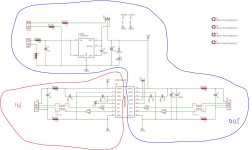
OK. Here is my drawing attached in a file.
As you can see four ground wires are attached to the ground only from one side and one ground wire is attached at both ends. That's all. There's nothing more to draw.
Your drawing does not show how you provide the power to each board. Also I assume there is a digital isolator on the USBI2S board. That needs power (VDD+GND) on both sides of the isolator. How is this provided.
I have standard and separate power supplies feeding the USB and the DAC board, transformer, diode bridge, capacitor, 78xx type regulator, capacitor.
As regards powering the USB board the digital part of the board is fed by PC power supply and the "clean" part is fed by a separate srandard power supply, i.e. transformer, diode bridge, capacitor, 78xx type regulator, capacitor.
Very simple and nothing special to talk about
As regards powering the USB board the digital part of the board is fed by PC power supply and the "clean" part is fed by a separate srandard power supply, i.e. transformer, diode bridge, capacitor, 78xx type regulator, capacitor.
Very simple and nothing special to talk about
Last edited:
Unfortunately all I can do is connect these 2 boards by wires only. No PCB, Sorry.Yes, those four are shield wires. They have poorly controlled impedance, and a discontinuity at the load.
This would work better if all the circuitry were on a single multilayer pcb.
And as I have been speaking above when I connect both ends of the four shield wires to the ground (which makes them ground wires) the quality deteriorates quite a lot.
Last edited:
How long are the I2S and ground wires? Where are the I2S and other ground wire in physical relation to transformers, power supplies, and their wiring? What is the physical orientation of the USB board ground plane relative the dac board ground plane, and what is the distance between them?
Look, there are good reasons we are asking for pics. This is RF we are dealing with. Some of the clock and data signals have risetimes that produce harmonic frequencies up to hundreds of MHz, and beyond. You don't have expertise in this area, you don't even have scope. So, if you want help then you should try to cooperate with the people willing to help you who have experience with weird RF problems like you have.
Look, there are good reasons we are asking for pics. This is RF we are dealing with. Some of the clock and data signals have risetimes that produce harmonic frequencies up to hundreds of MHz, and beyond. You don't have expertise in this area, you don't even have scope. So, if you want help then you should try to cooperate with the people willing to help you who have experience with weird RF problems like you have.
Last edited:
- Home
- Source & Line
- Digital Line Level
- proper grounding and shielding in i2s connection