I spotted these new choke/inductors in 17mm x 17mm packages.
An externally hosted image should be here but it was not working when we last tested it.
Datasheet
https://en.tdk.eu/inf/30/ds/b82599_a016.pdf
DCR typically under 10mO for 15uH
10% tolerance
12A saturation @ 20%. drop
Fairly flat to 7A
~ $5ea
More flat:
http://www.mouser.de/search/ProductDetail.aspx?R=0virtualkey0virtualkey7443630700
http://www.mouser.de/search/ProductDetail.aspx?R=0virtualkey0virtualkey7443631500
Much volume. Less space. The Wurth parts look good. Thanks. I spotted a few modders using them and the monstrous coil craft parts.
If I'm right, the STA516BE in BTL at 50v/6ohm = 7.4A = 165W @ 1% THD.
Any real reason to seek flat inductance beyond 7A ? The Wurth parts are 30% larger.
Last edited:
Your speakers impedance isn't 6R over the full bw. If it goes under 6R, more current will flow, resulting in some "core flux modulation distortion".
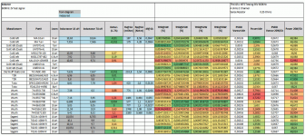
Some data from the TPA3251 Evaluation regarding inductors used in the output filter.

TDK ERU20 is also on the list, which is one size bigger than your posted ERU16 inductors.
Some data from the TPA3251 Evaluation regarding inductors used in the output filter.
TDK ERU20 is also on the list, which is one size bigger than your posted ERU16 inductors.
Attachments
Last edited:
Thanks DrMord.
I've picked up a second hand and recently calibrated UPL16 with 96khz board. I hope to test some of these things early next year when I have learnt how to use it! Edit : thanks for the chart!
I've also read the data sheet and application notes for the STA5xx series. What's you're opinion on differential as opposed to common mode snubbers before and after the inductor? ST favour common mode but give no evidence to back this decision. I've had a read of
IRF Class D Amplifier Basics but I'm none the wiser at the moment!
Just been brainstorming so far with layout. I have spotted the Keytstone 5102 jumper smd parts as a way to keep the ground plane as large as possible.
http://www.mouser.com/ds/2/215/102-743714.pdf
Here's the state of the STA516BE so far.
An externally hosted image should be here but it was not working when we last tested it.
Last edited:
I've got my eye on the STA311B. Although i'm working on a way to implement the Intersil D2-71083-LR (stand alone or HD Audio Interface over USB-C + PWR ) --> multi channel PWM. That may well require a group buy. I was thinking a D2 on dimm module exposing spdif, adc, tdm and pwm.
I've been reviewing D2audio DSPs. One of the neat features is PWM output (PUMPHI/PUMPLO) for power stage supplies and also a PSSYNC for synchronising switcher supplies. There are also a bunch of I/O for current and voltage protection/monitoring.
The EPC9203 is a compelling little dc-dc board with half bridge on board. I think I could generate a negative rail pump with this using the PWM from the DSP. http://epc-co.com/epc/documents/guides/EPC9203_qsg.pdf
The EPC9203 is a compelling little dc-dc board with half bridge on board. I think I could generate a negative rail pump with this using the PWM from the DSP. http://epc-co.com/epc/documents/guides/EPC9203_qsg.pdf
Last edited:
I really like what JL did with the D2audio dsp. The software looks great...
https://jlaudio.zendesk.com/hc/en-us/articles/218526388-TwK-Input-Mixer-Router-Basics
https://jlaudio.zendesk.com/hc/en-us/articles/218526388-TwK-Input-Mixer-Router-Basics
I wonder about which parameters may influence the sonic signature. I feel comfortable with the STA311 / STA5xx combo as the lower power STA326 and associated STA range have been recognised of very good performances.
From my perspective, going to a different signal processor, like the D2, may be jumping in the unknown with the associated risks (possibly better or worse).
My functional understanding of the thing, would be to build a big STA326, with more power and possibility to assemble easily a multichannel configuration: 2x2, 3x2. Easily accessible I2C configuration ports and I2S inputs. Sound design not cutting corners on those small things that tweakers have to do afterward and are not so costly if done right from the beginning.
But I would understand that it would not be your target.
By the way, it is nice to see all the things you explore !
JMF
JMF
Thanks JMF.
If I were to make a DSP board with PWM driving capabilty I would probably choose the D2. The ST range has no time delay functions.
For the D2 - Audio Canvas III looks like a great app.
Audio Canvas™ III | Intersil
The D2 range look fairly simple really. They have a built in DIT and DIR. You also have access to TDM so you can daisy chain and also HDA interface for interfacing to Windows sound systems. Here's sort of what I would lay out.
There are not many components here at all. It could be a fairly compact board.
There are a couple of D2Audio ICs at Mouser with MOQ=1 such as the older D2-92683-QR @ $10.
http://www2.mouser.com/ProductDetail/Intersil/D2-92683-QR/?qs=sGAEpiMZZMv1cXVJl98d9bjhQpaRcR6w
If I were to make a DSP board with PWM driving capabilty I would probably choose the D2. The ST range has no time delay functions.
For the D2 - Audio Canvas III looks like a great app.
Audio Canvas™ III | Intersil
The D2 range look fairly simple really. They have a built in DIT and DIR. You also have access to TDM so you can daisy chain and also HDA interface for interfacing to Windows sound systems. Here's sort of what I would lay out.
An externally hosted image should be here but it was not working when we last tested it.
There are not many components here at all. It could be a fairly compact board.
There are a couple of D2Audio ICs at Mouser with MOQ=1 such as the older D2-92683-QR @ $10.
http://www2.mouser.com/ProductDetail/Intersil/D2-92683-QR/?qs=sGAEpiMZZMv1cXVJl98d9bjhQpaRcR6w
Last edited:
This looks like a nice little first project and look at Audio Canvas III.
http://www.mouser.com/ds/2/465/d2-45057-157-555279.pdf
Single IC for spdif or i2s -> dsp -> 2ch/25W/1%THD.
Internal processing limited to 48Khz. This might be ok to try with my Audio Nirvana Super 15s.
I'm continuing with the STA311B+STA516BE as a project anyway. Easy to implement and program.
http://www.mouser.com/ds/2/465/d2-45057-157-555279.pdf
Single IC for spdif or i2s -> dsp -> 2ch/25W/1%THD.
Internal processing limited to 48Khz. This might be ok to try with my Audio Nirvana Super 15s.
I'm continuing with the STA311B+STA516BE as a project anyway. Easy to implement and program.
Last edited:
Hi,
I will read the application note, to learn a bit more. I would also be interested to learn how you consider to go for the manufacturing of the board. Do you consider hand soldering those components or some other alternative?
JMF
I will read the application note, to learn a bit more. I would also be interested to learn how you consider to go for the manufacturing of the board. Do you consider hand soldering those components or some other alternative?
JMF
I've been reviewing D2audio DSPs. One of the neat features is PWM output (PUMPHI/PUMPLO) for power stage supplies and also a PSSYNC for synchronising switcher supplies. There are also a bunch of I/O for current and voltage protection/monitoring.
The EPC9203 is a compelling little dc-dc board with half bridge on board. I think I could generate a negative rail pump with this using the PWM from the DSP. http://epc-co.com/epc/documents/guides/EPC9203_qsg.pdf
This board basically forms a LGA module (Land Grid Array) soldering these to your base board can be tricky even with a proper reflow oven, also the complexity of the mother board in terms of thermal considerations would be quite costly with filled micro vias, better as stated to use a simpler solution.
Hi,
I will read the application note, to learn a bit more. I would also be interested to learn how you consider to go for the manufacturing of the board. Do you consider hand soldering those components or some other alternative?
JMF
QFNs and similar with thermal pads require firstly the correct solder paste screen to really get the optimum solder joint formation, especially for the thermal pad, this is often critical to the device operation. This will also require a well controlled reflow cycle to also get again the optimum joint formation, again the thermal pad being critical. The design of the PCB that the devices are going on is also quite critical for correct operation and to avoid thermal issues, this usually involves the use of thermal vias (filled and capped or unfilled) in the area of the thermal pad, connected to inner planes and a copper area on the rear of the board so that you get some thermal conduction. 2oz thickness copper planes (or plane) give the best option for spreading the heat from a device, far better than 1oz planes. Better to have these devices soldered properly than risk a bad joint and spend forever trying to get a module to work.
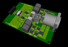
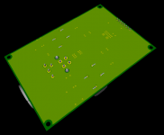
Work in progress. This is a 2ch PWM input board only at this time to be used with ongoing development of a 12 channel DSP board companion board.
More details and updates to follow.
Firstly, I'll be changing the inductors from ICE 14DA to Wurth 744363 as suggested by doctormord earlier. Then working on compacting the board and component layout.
More details and updates to follow.
Firstly, I'll be changing the inductors from ICE 14DA to Wurth 744363 as suggested by doctormord earlier. Then working on compacting the board and component layout.
Attachments
Last edited:
Does anyone have any advice on GND_CLEAN. Would this be best to use a ground trace off board?
GND_Clean
This pin is the reference GND for all input logic signals, so it must be as clean as possible. Is recommended not connect directly this GND with other GNDs (i.e. speaker GND) that are interested by voltage spikes.
GND_Clean
This pin is the reference GND for all input logic signals, so it must be as clean as possible. Is recommended not connect directly this GND with other GNDs (i.e. speaker GND) that are interested by voltage spikes.
Does anyone have any advice on GND_CLEAN. Would this be best to use a ground trace off board?
GND_Clean
This pin is the reference GND for all input logic signals, so it must be as clean as possible. Is recommended not connect directly this GND with other GNDs (i.e. speaker GND) that are interested by voltage spikes.
"Reference GND for all input signals" implies it must go together with logic signals wherever they go. If they go off-board, then GND must too. The question is how you connect it to other GNDs. "Not directly" is not a real suggestion. You must connect them somehow, this is clear, but the exact way may depend on the system, and the internal GND connections and separation capabilities of the IC. But basically if you do power decoupling well (this is not a trivial task at layout level) and you connect power GND to signal GND at only 1 place under the IC, then you have a good chance to avoid problems at this aspect. Logic level signal tracing is an other thing. Although it is digital, the timing errors in it are analogue by nature, and signal transition imperfections causes timing error (jitter). The jitter tolerance in such system is incredibly low if you want to achieve the theoretical resolution capabilities. Full scale: 2 us -> -100 dB = 20 ps. If you have eg. 100 mV uncorrelated disturbance during transition, and despite of this you want to limit timing error to 20 ps, then you need a signal slew rate of 5V/ns, which is achievable, but then you need impedance matched routing and significant track separation, (and high speed interconnect cables if modulator is on separate board). GND should not be a track. It must be a layer or a continuous polygon under all signal tracks.
1 GND pin per connector is not enough. The minimum is 1 GND between each signals. The better is shielded cable. Plus common mode filter ferrites on signal+GND pairs. And an RF optimized connector... and cable impedance matching to PCB and source.
- Status
- Not open for further replies.
- Home
- Amplifiers
- Class D
- Project Moshulu : a journey into class D