hello Marc,
I have done some layouting for triyng to achieve the goal of low stray inductance.
Original schematic is designed by MAG
Could you take a look at it?
The pcb misses decoupling caps from the high side drain to the low side source (need to draw the parts)
It is done in Express PCB (free software).
Thanks and regards,
Savu Silviu
Attachments
Last edited:
hello Markus,
We are still debating on the solution. for the time beeing is important to have the final layout, in order to take that decision. Marc is working hard on the layout.
Regards,
We are still debating on the solution. for the time beeing is important to have the final layout, in order to take that decision. Marc is working hard on the layout.
Regards,
Isn't this a simmilar idea: http://www.amplifier.co.uk/images/SDV1025-300_1_ETS.pdf ?
It looks like 4 output devices (D2-PAK package) can deliver 300W without a heatsink.
Could you provide a space for 4 output transistors?
Mark
It looks like 4 output devices (D2-PAK package) can deliver 300W without a heatsink.
Could you provide a space for 4 output transistors?
Mark
It is a similar one but our project will use PQFN devices they measure 5mm / 6mm / 2mm (height).
The amp in the PDF is realy good but it lacks a ground plane.
true class d amps have at least 2 ground planes.
After we test the transistors in harlbridge I will try also a fullbridge prototype.
Regards,
The amp in the PDF is realy good but it lacks a ground plane.
true class d amps have at least 2 ground planes.
After we test the transistors in harlbridge I will try also a fullbridge prototype.
Regards,
Hi
sorry about any delay, but been busy at work, as well as revting the output section of the amp. Where most of EMC prblrms are quite often caused by bad layot.
So after looking at xamplelyouts varios data sheets and application notes and a few changes, I am pretty shur I,v got the output section close. The two main criteria where low inductance loops for switching circuits and copper areas for thermal management.
Attachments
Forgot, currently about 108x74mm (4 x 3 inch), the file 1to1-A4-pdf.pdf is a 1:1 image of the top layer that when rpinted A4 shows actual size.
The other two are top and bottom copper (in grey) with component placement superimposed on top. he clear holes in the copper are the drill locations fot the vias (both thermal and electrical).
Appologie, havent had time to download PCB express yet Savu, will try tommorow (had to take daughters shopping today! ).
May I suggest adding mounting holes in corners of the board?
What is the expect power of the amp?
Would it help if you add another pair of the output devices (there is a lot of space on the board)?
Mark
What is the expect power of the amp?
Would it help if you add another pair of the output devices (there is a lot of space on the board)?
Mark
Hi,
there will eventualy be at least six mounting holes. The idea being to aid heat dissipation the board can be monted to either an ali block, case or heatsink using somthing similar to:
Thermal Materials, Thermal Solutions ~ The Bergquist Company
http://www.bergquistcompany.com/the...d/pdfs/gap-pad-vo-soft/PDS_GP_VOS_12.08_E.pdf
this will help disperse the heat, and quite effectivly. My initial idea would be to try just a flat 4 or 5mm thick block of aluminium. Any metal used this way will have to be fastened to a safety earth directly at a single point, and holes drilled to allow clearance for through hole pins.
The room available at the output end has been dictaed by the large output caps and res. There is room for either doubling up the output devices, a good idea as it also spreads the heat generated, or looking at shrinking the circuitry. The one advantage is does give is plenty of copper to get rid of the heat, off the top of my head 2 square inch of 1oz FR4 is approx 16-20deg C/W.
I'd like to build it. Mainly because the board is do nicely designed by Marce (and to see whether the amp works 🙂). It's a pitty that it has no protection circuit. Is it possible to add at least short circuit protection, or is it too late for such a modification?
Mark
Mark
I'd like to build it. Mainly because the board is do nicely designed by Marce (and to see whether the amp works 🙂). It's a pitty that it has no protection circuit. Is it possible to add at least short circuit protection, or is it too late for such a modification?
Mark
Hello Mark,
The schematic of the amp works. The purpuse of this thread is too see if the IRFH5020 and IRFH5015 have good result for class d amp. After the amp is built and everything is measured i will start work on a class D amp using these transistors to their limit.
For the moment we have to test the transistors behaviour in a class D amp.
Regards,
Savu Silviu
Will be doing the other part of the layout after work tonite.
I also want to build this as I have two H-frame 15" sunbwoofers that need amps.
Once I've done the layout I've quite a lot of thoughts etc on construction etc which I would like to discuss.
I also want to build this as I have two H-frame 15" sunbwoofers that need amps.
Once I've done the layout I've quite a lot of thoughts etc on construction etc which I would like to discuss.
Almost done:
Got the 12V supply to finalise.
There is room to shrink the board down, probably to around 95mm x 68mm.
Sorry things are apearing in little bursts, but its mayhem at work, 7 days a week at the moment, so I never seem to have any spare time, we'll be back to normal soon though I hope!
When I get some more time I want to have a look round at components as I saw some Vishay 2W resistors that are nearly half the size of the ones on the board now (RD1 & RC1). Also maybe using two smaller electrolytics for CJ1 & CH1.
I am a lot happier with this design now and since moving everything around it all gels together much nicer.
Hello Marc,
sorry for the fact that I am short in posting but I have a lot of problems to solve at work so I work minmum 12 hours a day 7 days per week.
when toyota will cool down a bit with the new yaris project i'll be back in bussiness.
regards,
sorry for the fact that I am short in posting but I have a lot of problems to solve at work so I work minmum 12 hours a day 7 days per week.
when toyota will cool down a bit with the new yaris project i'll be back in bussiness.
regards,
Were both in the same boat, were designing boards etc like mad for our BIGGEST ever contract, and as its gonna guarantee work for 5 plus years, I consider the sacrifice worth it.
Good news, I'm off work tommorow so I can finaly finish the layout.
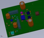
To cater for the mechanical side I've been playing with the IDF (Intermediate Data Format), Circuitworks and Solid Works to start creating the 3D assembly for the board.
A overview of the IDF transfer:
www.aertia.com/docs/priware/CircuitWorks7.ppt
The IDF 3.0 spec (currently the only full version supported by most ECAD and MCAD packages:
http://www.simplifiedsolutionsinc.com/images/idf_v30_spec.pdf
I've attached a screen shot of the assembly so far, I still have to model some of the PTH components. The advantage of using this form of transfer between the PCB layout package and a 3D package such as Solid Works is in fitting the board into an enclosure, or if doing a custom enclosue, designing the enclosure around the PCB assembly.
Attachments
The other advantage is being able to produce some quick and quite nice assembly drawings. On think I do with prototypes is print the drilling info onto A4 sized labels that you can then align and stick on the board to provide location points for drilling.
When the assembly is completed I will either create a parasolid of the assembly or use the pack and go function so your freind who has SW has all the mechanical data.
A quick example of the derived drawings from an IDF-Solid Works assembly. The only thing that dosn't transfer easily are the component references, it is possible to transfer them but is a pain to get them to apear on the drawings.
P.S I havn't forgoten the mounting holes.🙂
Attachments
- Status
- Not open for further replies.
- Home
- Amplifiers
- Class D
- PQFN 5X6mm Packaged N channel Power Mosfet in ClassD ...