I can confirm that my build of NMOS200 works. I have used one pair IRFP460, rails are at 40V. Quiscent bias is quite fine (40mA) and DC offset is less than 10mV.
Mine too with IRFP450 since many yearsI can confirm that my build of NMOS200 works. I have used one pair IRFP460, rails are at 40V. Quiscent bias is quite fine (40mA) and DC offset is less than 10mV.
http://audiyofield.wifeo.com/mnos-200.php
I have only one problem - there's hum. Only if I ground the input, it's gone. So I presume there some kind of ground loop including amp and preamp.
Hi Rankot, what has worked for me in the past is connecting the pre-amp chassis to the power amp chassis with a jumper wire. This puts both chassis at the same potential.
Cheers
Cheers
Bonsai has made a good guide on how to manage ground with clear drawings
For dual mono blocs : https://hifisonix.com/how-to-wire-up-a-dual-mono-bloc-amplifier/
and more general on ground loops and shared power supply in stereo amp : https://hifisonix.com/ground-loops/
For dual mono blocs : https://hifisonix.com/how-to-wire-up-a-dual-mono-bloc-amplifier/
and more general on ground loops and shared power supply in stereo amp : https://hifisonix.com/ground-loops/
Thanks for responses. My preamp is actually in the same chassis as the amp (it is a bass amp), and actually disconnecting ground wires from PS to preamp and from preamp output to amp input reduced hum a lot. Their grounds are now connected through chassis, by in/out jacks only. I will try to put isolated jack for speaker output, to see what happens. I don't have a ground lift there, so maybe that is a problem?
Neither input nor output ground should be connected to the chassis.
Bonsai's writeup mentioned above is very good, if you follow his instructions there should be no hum.
Bonsai's writeup mentioned above is very good, if you follow his instructions there should be no hum.
Hello!
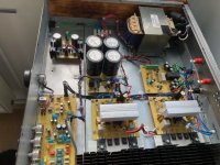
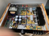
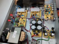
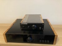
I also managed to finish the N-MOS 200 amplifier.
It sounds great.
Thank you Quasi for sharing this great project.
This is what my version looks like.
I also managed to finish the N-MOS 200 amplifier.
It sounds great.
Thank you Quasi for sharing this great project.
This is what my version looks like.
Attachments

Hi Marin,
Very neatly laid out - very professional. I like the layout of the various modules, well thought out. Nice case too.
Glad you like the performance - happy listening.
Cheers
Q
Very neatly laid out - very professional. I like the layout of the various modules, well thought out. Nice case too.
Glad you like the performance - happy listening.
Cheers
Q
Hi Quasi,
I want to make a Nbip amp with one pair of BJT output at +- 35v DC. Can you propose a schematic for this amp?
Thanks in advance.
Alain
I want to make a Nbip amp with one pair of BJT output at +- 35v DC. Can you propose a schematic for this amp?
Thanks in advance.
Alain
Hi @quasi ,
I am reading through the "...under construction" thread for a while now during coffee breaks and am fascinated by the traction your design had over time.
Just recently I learned about the "Brother of Quasi" with BJT as output stage.
In LTSpice, both versions look very promising.
Because both schematics are very similar, I am thinking about creating one layout / PCB and use for both. I will strip down the BoQ to use only two output devices in TO247 / TO-3P, like the Nmos200. For power supply, I will use +/30V. I know that your original intention was for high power, but with these parameters, I am still getting about 65W RMS into 4 Ohms. Having 90 dB speakers (and about to build 97 dB ones) I do not think I need more (currently listening to a 7W tube amp and that has plenty of power with my speakers).
For power FETs: I somehow stumbled upon the IRFP264, which in the sim has a much better THD behaviour than the IRFP450. Not sure if that really means anything, or is really true in reality, though. I might still gave that a try.
Some smaller questions:
1) In the BoQ, there are a diode and 33nF capacitor in parallel to one of the resistors in the driver stage. What are they for?
2) In some schematic variation I currently cannot find again, there also was a diode (1N914) between the collectors of the long-tail pair? Why?
3) Somewhere you said R7, the resistor in the long-tail pair should be 4k7 for lower rail voltages. Why is that? In the sim, this seems to make no diff.
Thanks,
Mo
Last edited:
Try to reverce the position of the amplifier input capacitor.I have only one problem - there's hum. Only if I ground the input, it's gone. So I presume there some kind of ground loop including amp and preamp.
Hi @quasi ,
I am reading through the "...under construction" thread for a while now during coffee breaks and am fascinated by the traction your design had over time.
Just recently I learned about the "Brother of Quasi" with BJT as output stage.
In LTSpice, both versions look very promising.
Because both schematics are very similar, I am thinking about creating one layout / PCB and use for both. I will strip down the BoQ to use only two output devices in TO247 / TO-3P, like the Nmos200. For power supply, I will use +/30V. I know that your original intention was for high power, but with these parameters, I am still getting about 65W RMS into 4 Ohms. Having 90 dB speakers (and about to build 97 dB ones) I do not think I need more (currently listening to a 7W tube amp and that has plenty of power with my speakers).
For power FETs: I somehow stumbled upon the IRFP264, which in the sim has a much better THD behaviour than the IRFP450. Not sure if that really means anything, or is really true in reality, though. I might still gave that a try.
Some smaller questions:
1) In the BoQ, there are a diode and 33nF capacitor in parallel to one of the resistors in the driver stage. What are they for?
2) In some schematic variation I currently cannot find again, there also was a diode (1N914) between the collectors of the long-tail pair? Why?
3) Somewhere you said R7, the resistor in the long-tail pair should be 4k7 for lower rail voltages. Why is that? In the sim, this seems to make no diff.
Thanks,
Mo
Hi Mo,
Sorry abut the late reply. Answers below.
1) In BoQ the positive rail driver transistor (T9) forms a Darlington configuration with the output stage. The Vbe for darlingtons is typically 1.2 volts.
The negative rail driver (T10) forms a Sziklai Pair with the output stage. Sziklai Pair Vbe is typically 0.6 volts, so a diode is added to improve DC symmetry by dropping another 0.6 volts. The resistor and capacitor improve distortion and clipping symmetry.
2) In the ACTRK amplifier series there are anti-parallel diodes across the collectors of the LTP. These are to prevent the amplifier latching to one rail during abnormal signal or operating conditions. This actually can happen (it did to me with pretty bad results). The diodes stop this happening.
3) For lower voltages R7 should be reduced so there is enough voltage across T2 to work as a constant current source (CCS). The configuration of T2, R8, D4 & D5 plus R12 work to provide a CCS of about 1.8 mA. This current x 4k7 = 8.5v leaving 21.5 volts across T2 with your 30v rails.
As for the IRFP264 having lower THD than the IRFP450 I cant comment. Note though that the IRFP264 has a higher input capacitance; 3860 pF versus 2600 pF so plotting a sim at higher frequencies might be worthwhile. As for the real world - who knows!
Cheers
Q
Hi Quasi, thanks for the detailed answers.
2) a) Can these situations only happen with the ACTRK? Or should I include such diodes for safety also in PCBs for the NMOS and BoQ?
2) b) The variant I mean was slightly different, it had only one diode of type 1N914. Likely this was somewhere along the road in the thread. It is not in the latest versions of any variant, so I will just ignore.
3) At least in the sim, 7k vs. 10k results in 2.41 vs. 2.4 mA.
At 100k, output does not drop significantly in the sim. At 100k the output is down by about 0.45 dB in the simulation compared to 1k. THD at 100k is about 1.8% for 1W RMS. With the other FET
4) (New question) How do I calculate the "best" bias current per FET for the different options? I think you suggested about 30mA per FET pair in the construction guide. When going higher (like 100mA per FET), THD significantly drops in the sim.
For AB I absolutely have no clue about this.
Thanks,
Mo
2) a) Can these situations only happen with the ACTRK? Or should I include such diodes for safety also in PCBs for the NMOS and BoQ?
2) b) The variant I mean was slightly different, it had only one diode of type 1N914. Likely this was somewhere along the road in the thread. It is not in the latest versions of any variant, so I will just ignore.
3) At least in the sim, 7k vs. 10k results in 2.41 vs. 2.4 mA.
quasi said:Note though that the IRFP264 has a higher input capacitance; 3860 pF versus 2600 pF so plotting a sim at higher frequencies might be worthwhile.
At 100k, output does not drop significantly in the sim. At 100k the output is down by about 0.45 dB in the simulation compared to 1k. THD at 100k is about 1.8% for 1W RMS. With the other FET
4) (New question) How do I calculate the "best" bias current per FET for the different options? I think you suggested about 30mA per FET pair in the construction guide. When going higher (like 100mA per FET), THD significantly drops in the sim.
For AB I absolutely have no clue about this.
Thanks,
Mo
Hi Mo
2) a) Can these situations only happen with the ACTRK? Or should I include such diodes for safety also in PCBs for the NMOS and BoQ?
The Nmos and BoQ did not exhibit this so no need for the diodes.
3) At least in the sim, 7k vs. 10k results in 2.41 vs. 2.4 mA.
You are correct. I did my calculations using a slightly earlier schematic. Depending on the Vbe of the CCS transistor the current should be between 2.3 and 2.7 mA. In this instance the CCS components are T4, D1 & D2, R8 and R11. I would use 8k2 for R7. This will drop about 20v leaving 10v for T4.

Cheers
Q
2) a) Can these situations only happen with the ACTRK? Or should I include such diodes for safety also in PCBs for the NMOS and BoQ?
The Nmos and BoQ did not exhibit this so no need for the diodes.
3) At least in the sim, 7k vs. 10k results in 2.41 vs. 2.4 mA.
You are correct. I did my calculations using a slightly earlier schematic. Depending on the Vbe of the CCS transistor the current should be between 2.3 and 2.7 mA. In this instance the CCS components are T4, D1 & D2, R8 and R11. I would use 8k2 for R7. This will drop about 20v leaving 10v for T4.
Cheers
Q
Thanks Quasi.
What about the biasing? I think you somewhere said like 30mA per FET pair. With about 10x as much, THD level and distribution (even vs. odd harmonics) is improved a lot.
Expectedly that consumes more current, but 20W vs. 16W power need per channel at 1W RMS is not that much worse. Idle is more different with 14W vs. 3W, but nothing against class A.
So, how to find the "ideal" bias in these AB designs?
Thanks, Mo
Hi Mo, because your voltage is lower you can increase the bias current. At 100mA you would still be only 3 watts per output device and probably achieve good distortion figures. I found that FETs generally need more bias than transistors in output stages.
Trying to find the ideal bias? Don't know other than a bench set-up where you can experiment.
Cheers
Q
Trying to find the ideal bias? Don't know other than a bench set-up where you can experiment.
Cheers
Q
- Home
- Amplifiers
- Solid State
- Power amp under development