Hi Vu,
sorry, sometimes I forget we don't all have English as our native language and worse I used an acronym.
NFB= Negative FeedBack, in this case the global NFB loop.
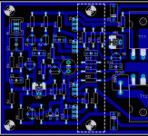
The link to a resistor at the left hand end of the wide output trace looks like the NFB tapping point that returns a proportion of the output voltage to the inverting input.
no, C5 & C6 and R2 but I can't read these clearly.
sorry, sometimes I forget we don't all have English as our native language and worse I used an acronym.
NFB= Negative FeedBack, in this case the global NFB loop.
The link to a resistor at the left hand end of the wide output trace looks like the NFB tapping point that returns a proportion of the output voltage to the inverting input.
no, C5 & C6 and R2 but I can't read these clearly.
What transistor should I use for T8 if I don't like BC546 ?
I want something like MJE to hold it with a screw... 😕
MJE340 it's good ? or has lower amplification ? or doesn't matter ? 😀
I want something like MJE to hold it with a screw... 😕
MJE340 it's good ? or has lower amplification ? or doesn't matter ? 😀
Re: Re: Re: Warning - Nmos200
Hi Quasi,
Thanks for the explaination. Would it be appropriate to list R11 on your Power Selection Guide as well to show the R11 value vs rail voltage?
Regards,
John L. Males
Willowdale, Ontario
Canada
31 August 2007 08:24
Official Quasi Thread Researcher
quasi said:
R11 provides some bias to turn diodes D1&D2 on. These diodes set a voltage of around 1.2 volts which is the reference for the two constant current sources T4 & T7.
It was always my intention to have this at 22K for the Nmos200 and this is the value I used in the PCB layout, but forgot to change it in the schematic. The reason I lowered it from 27K as used in the Nmos350 / 500 was to maintain sufficient current with the generally lower rail voltages suggested for the Nmos200.
This resistor is not related to the feedback or input part of the schematic at all. Indeed it has nothing to do with the signal path.
Cheers
Q
Hi Quasi,
Thanks for the explaination. Would it be appropriate to list R11 on your Power Selection Guide as well to show the R11 value vs rail voltage?
Regards,
John L. Males
Willowdale, Ontario
Canada
31 August 2007 08:24
Official Quasi Thread Researcher
Hi Marus,
almost any To126 device will do.
Ft between 50MHz and 200MHz
hFE between 100 and 400
Vce0 >12V
Why do you not like bc To92 part?
almost any To126 device will do.
Ft between 50MHz and 200MHz
hFE between 100 and 400
Vce0 >12V
Why do you not like bc To92 part?
Hi Vu,
r21 MUST sample the speaker output.
Somewhere near the output Thiele network would be a suitable tapping point. But, I think it must be before the output coil/inductor.
r21 MUST sample the speaker output.
Somewhere near the output Thiele network would be a suitable tapping point. But, I think it must be before the output coil/inductor.
Hi,
how quickly will a To126 respond compared to a To92?
Why don't you try glueing the To92 with that instant (60second) glue that is so thin that there is almost no thermal resistance across the interface. But there must be no air in the interface.
The To126 must be electrically isolated from the heatsink or attached to the insulated face of one of the output devices.
Hari,
RegardingPost #2249 and nmos 160a.pdf I have discovered these initial issues that may uncover more issues:
1) Your nmos 160a.pdf R17 and R18 appears to be R18 and R19 respectively on the NMOS200 schematic.
2) Your nmos 160a.pdf R19 appears to be R17 on the NMOS200 schematic.
3) Your nmos 160a.pdf R17 (appears to be R18 respectively on the NMOS200 schematic) has a link that ends near R31 looks orfaned with the move of L1 to to the C13 side of PCB. That link I believe should be at the L1/R35 PCB node.
4) Your nmos 160a.pdf R11 still shows 27K0 on the PCB silkscreen, and should be 22K per quasi's Post #2230 and Post #2239.
Excellent moving of C7B to avoid T7 thermal coupling to C7B, and the centering T8.
Big thanks for putting up with my observations/comments.
Regards,
John L. Males
Willowdale, Ontario
Canada
31 August 2007 (22:00 -) 22:54
Official Quasi Thread Researcher
keypunch said:Hari,
RegardingPost #2249 and nmos 160a.pdf I have discovered these initial issues that may uncover more issues:
1) Your nmos 160a.pdf R17 and R18 appears to be R18 and R19 respectively on the NMOS200 schematic.
2) Your nmos 160a.pdf R19 appears to be R17 on the NMOS200 schematic.
3) Your nmos 160a.pdf R17 (appears to be R18 respectively on the NMOS200 schematic) has a link that ends near R31 looks orfaned with the move of L1 to to the C13 side of PCB. That link I believe should be at the L1/R35 PCB node.
4) Your nmos 160a.pdf R11 still shows 27K0 on the PCB silkscreen, and should be 22K per quasi's Post #2230 and Post #2239.
Excellent moving of C7B to avoid T7 thermal coupling to C7B, and the centering T8.
Big thanks for putting up with my observations/comments.
John
You sure have gone through the layout in great detail. Thanks a ton for doing so. But you seem to have forgotten, I'm using the nmos350 schematic and not the nmos200. In fact, the two are same except for the component values.
I've moved the wire link also to the right side, its for the NFB.
Thanks again for cleaning up my design.
Cheers
Hari
Hi Hari,
Yes you are correct I was referencing the NMOS200 scehmatic. I thought, though it had been a while, the part numbers of the NMOS350 and NMOS200 were the same at least to the driver stage. Clearly my "aging" memory was incorrect.
Regards,
John L. Males
Willowdale, Ontario
Canada
01 Sept 2007 09:22
Official Quasi Thread Researcher
Hi Hari,
I only have a few minutes right now to look over "today's version of my pcb layout".
You may want to move the rectangle for the L1/Output node a bit more away from C13. The main reason for the suggestion is to reduce ark potiential and also allow a bit more room to make the connection to the output terminal. I am only suggesting moving the large pad. The size and dimension is just fine.
The "OUT" text was left over VPOS track that should of been moved when the L1/Output pad were moved to the C13 side of the PCB.
I really have not spent any time checking the parts/nodes to see if all is in order. It may of seemed like I had with my last comments, but it was driven by the stray under PCB link that you have corrected that caused me to make the part numbering comments I had as I tried to figure out if the stray link was still required.
Regards,
John L. Males
Willowdale, Ontario
Canada
03 Sept 2007 (20:40 -) 21:27
Official Quasi Thread Researcher
Hi AndrewT,
You can help me, because I can't find transistor BC556/546 in VietNam. Can I change by 2SC1815/2SA1015? and IRFP450 --> IRFP240.
Thank you vey much
You can help me, because I can't find transistor BC556/546 in VietNam. Can I change by 2SC1815/2SA1015? and IRFP450 --> IRFP240.
Thank you vey much
Hi Vu,
I cannot comment on the FET substitutuion.
as for the 1015/1815 substitution.
Where?
The Vce0 has gone from 60Vce0 to 50Vce0.
The gain varies a lot 70 to 700.
One end of the range suits some locations and the other end of the range may be better in others.
I cannot comment on the FET substitutuion.
as for the 1015/1815 substitution.
Where?
The Vce0 has gone from 60Vce0 to 50Vce0.
The gain varies a lot 70 to 700.
One end of the range suits some locations and the other end of the range may be better in others.
Hi vuthanh6,
Quasi did mention it before that irfp240 can be used instead of irfp450. I don't remember it was in the thread or a private feedback to me.
BTW, did anyone use a TO-126 (or other flat) package for T8 and what exactly did you use? I am worried how to make it fit (TO-92) into the heatsink.
Quasi did mention it before that irfp240 can be used instead of irfp450. I don't remember it was in the thread or a private feedback to me.
BTW, did anyone use a TO-126 (or other flat) package for T8 and what exactly did you use? I am worried how to make it fit (TO-92) into the heatsink.
http://www.audio-electronics.go.ro
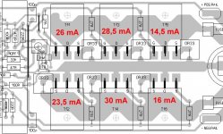
I finished the second channel ... 😀
Someone please tell me if i'm right with the secifications ?
I finished the second channel ... 😀
Someone please tell me if i'm right with the secifications ?

Hi,
did you measure and match the source resistors?
If they are +-10% tolerance then that could account for upto 20% of your variation.
The remainder of this enormous variation is due to using unmatched FETs.
In a stereo pair one would have 12FETs. These can be arranged in four groups of three. Each group of three are inserted in either the upper half or the lower half of the PCBs.
- Home
- Amplifiers
- Solid State
- Power amp under development