Hi Quasi,
the Zeners should connect gate to source. They can be sized to do either gate protection or to double up as short circuit protection.
The 27r limits the current into each Zener and limits the current from the drivers in a fault situation, until the fuses blow.
What value of gate resistors are needed to ensure that the proposed Zeners and T9/10 survive?
If the Zeners are connected direct to gate & source, will this cause oscillation of the output FETs?
If T9 & T10 are at risk, then why not add current limiters to protect the VAS & drivers?
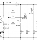
my idea of conecting zener diodes into the NMOS350 was to split the gate resistor in two pieces and between the two resistors connect the the cathode of the zener diode, the anode will be connected to the output of the amplifier.
This configuration will protect T9 and T10 and will also protect the output stage as the voltage drop across source resistors caused by the large currents flowing through the load will be substracted from the gate-source voltage limiting the output power. I agree that will introduce some distorsions in the output signal but this will only happend at high power levels..... i think
I attached a small schematic to explain what i mean.
Attachments
Hi all
I finally managed to create the pdf file of my pcb layout (nmos350) in under 100Kb size. Please do go through this with a tooth comb and give me your feedback.
John (keypunch), thanks a million for your tips on creating a smaller pdf file. I have also incorporated the changes that you suggested in the layout.
Hari
Attachments
AndrewT said:Hi, decide your safe output current for each device in the output stage. Look up the datasheet and select the voltage from the Vds vs Id graph that matches your maximum current.
Don't forget tp take temperature into account!
In general, less Vgs is needed for given Id as temperature rises, but this tendency itself is lower as Id rises, if we assume vertical MOSFETs. In general, the temperature co-efficient is about zero close to the maximum MOSFET current, +0 -3 dB 🙂
The problem with this method is that the Vds vs Id is not straight horizontal line. As Vds rises so does Id leading to a compromise; higher dissipation than the device can take versus adequate pass current without hitting the limiter. This becomes very significant into reactive loads where High Vds can co-exist with High Id.
The result is audible limiting, or inadequate protection. Take your choice.
Zener limiting in geenral works much better in cases where there is a source resistor. Normally, it is there to enable current sharing between parallel MOSFETs, and as MOSFETs have relatively low gm, the resistors are of relatively high value, compared to what one would find in BJT outputs. Resistors are often 0.33..0.5 ohms. At klimiter currents, there will be a seizable voltage drop on the source resistor, so much so that it overwhelms the Vgs tolerances, which is indeed what the resistor is for. In such a system zener limiting can be quite precise.
My experience with it is that I have never had stability problems when the zener was on the MOSFET gate side of the gate damper resistor. Even so, the damper resistor itself is a compromise and often does not guarantee any protection of the VAS transistor(s). It is actually very common to see protection circuits like the one earlyer in the thread, grafted onto completely overcurrent unprotected VAS designs, probably by knee-=jerk reflexive copy-paste.
I also have experience with zener protection where there are no source resistors. This is usually very tricky business as you can only match a few MOSFETs to the available zeners and required maximum current.
In general it has been my experience that MOSFETs are indeed robust enough to survive fuses if the current is properly limited, and of course, the proper fuses are chosen (aside the problem that it is not always trivial to decide where in the output circuit the fuses should go, to produce the least audible impact - remember, they are nonlinear resistors). Fuses must be fast acting, and dimensioned for half the effective value of current into the lowest expected resistive load. MOSFETs on the other hand should be capable of 2-3 times the fuse current, and this peak should fall inside the SOA curve for one half period of the lowest expected output frequency. Needless to say, this is not easy to satisfy... in general, if in doubt, you need to add more parallel MOSFETs (or larger MOSFETs)... and keep watching the effective gate capacitances as you do so.
Hi Jethari,
can you add a film bypass to C7?
Rotate Q5 to face Q1. Close couple for thermal matching.
How about adding a fourth pin pad just like KSA Klone to allow either BC or 2sa types for the LTPs
can you add a film bypass to C7?
Rotate Q5 to face Q1. Close couple for thermal matching.
How about adding a fourth pin pad just like KSA Klone to allow either BC or 2sa types for the LTPs
AndrewT said:Hi Jethari,
can you add a film bypass to C7?
Rotate Q5 to face Q1. Close couple for thermal matching.
How about adding a fourth pin pad just like KSA Klone to allow either BC or 2sa types for the LTPs
Andrew
Thanks for the reply, quick work!
Film bypass for C7 - would it just one cap or one for each electro cap?
Rotate Q5 - just did that, had to add a wire link for the emitter.
Fourth pin pad - what are LTPs?
Thanks
Hari
Hi,
single bypass cap across the series pair of electros.
You don't need a wire link for the emitter. You can also fit four pads ebce and still not need a link.
LTP=long tail pair=differential input.
Add multiple pin pitch to the caps where you have room.
single bypass cap across the series pair of electros.
You don't need a wire link for the emitter. You can also fit four pads ebce and still not need a link.
LTP=long tail pair=differential input.
Add multiple pin pitch to the caps where you have room.
AndrewT said:Hi Quasi,
the Zeners should connect gate to source. They can be sized to do either gate protection or to double up as short circuit protection.
The 27r limits the current into each Zener and limits the current from the drivers in a fault situation, until the fuses blow.
What value of gate resistors are needed to ensure that the proposed Zeners and T9/10 survive?
If the Zeners are connected direct to gate & source, will this cause oscillation of the output FETs?
If T9 & T10 are at risk, then why not add current limiters to protect the VAS & drivers?
cd-i said:my idea of conecting zener diodes into the NMOS350 was to split the gate resistor in two pieces and between the two resistors connect the the cathode of the zener diode, the anode will be connected to the output of the amplifier.
This configuration will protect T9 and T10 and will also protect the output stage as the voltage drop across source resistors caused by the large currents flowing through the load will be substracted from the gate-source voltage limiting the output power. I agree that will introduce some distorsions in the output signal but this will only happend at high power levels..... i think
I attached a small schematic to explain what i mean.
Splitting the gate resistors will work to a degree but the size of resistor required will compromise performance.
Some maths is in order.
Using a 7.5 volt zener and a 100 ohm resistor.
75 volts - 7.5v = 67.5 volts / 100 ohms = 675mA = 45 watts in the resistor and 5 watts in the zener. A 5 watt zener should survive until the fuses blow, but the resistor is already dead and the drive has been removed from the FETs. Hmmm...maybe this is one answer?
We could use a 1k0 resistor. Then we have 4.5 watts in the resistor and 0.5 watts in the zener, not too bad. But the impedance of the gate drive is now too high for good FET control.
I'm thinking about using low Rds-on FETs in the power supply feeds that will latch off in the event of an over-current situation.
Cheers
Q
Hi All,
Is all this discussion for short circuit protection about devices, output devices specifically, that will blow before the rail fuse(s) in a output short condition? If so, is the damage to the devices caused by going over the thermal limits of the output devices due to the obvious current draw affecting Tj and exceeding the device SOA?
Regards,
John L. Males
Willowdale, Ontario
Canada
12 July 2007 08:48
Official Quasi Thread Researcher
AndrewT said:Hi,
single bypass cap across the series pair of electros.
You don't need a wire link for the emitter. You can also fit four pads ebce and still not need a link.
LTP=long tail pair=differential input.
Add multiple pin pitch to the caps where you have room.
Andrew
I dont seem to be able to find a footprint for a four pad transistor. I might have to do manual drawing of the footprint.
I've included the bypass cap for C7. A 0.1uF should do well wont it?
Hari
Hi,keypunch said:Is all this discussion for short circuit protection about devices, output devices specifically, that will blow before the rail fuse(s) in a output short condition? If so, is the damage to the devices caused by going over the thermal limits of the output devices due to the obvious current draw affecting Tj and exceeding the device SOA?
the SOA shows an absolute current limit (the horizontal line) out to a defined maximum voltage. At this first knee the device is at a thermal limit in the silicon die area.
To the right of the knee the die is still at a thermal limit.
To the left of the knee the manufacturers usually state that the bonded wires to the external legs are the limiting factor. It would appear that it is not Tj that sets the current limit but the bonding wires when the voltage is below that first knee. For vertical FETs the drain is connected to the die, so this limit is more likely to be a source leg current limit which will be connected by a bonding wire.
Some devices show a range of absolute current limits depending on the duration of the pulse, but this more often applies to smaller devices.
Hi,jethari said:I don't seem to be able to find a footprint for a four pad transistor. I might have to do manual drawing of the footprint.
I've included the bypass cap for C7. A 0.1uF should do well won't it?
you won't find a 4pad transistor.
Have a look at the Krell ksa100 clone to see what it looks like. It appears the designer placed two transistors on top of each other to create the 4pads, but you could just a easily manually create a fourth pad (extra emitter) and link it across with a trace. It leaves the option to use either CBE or BCE for the input pairs.
http://www.diyaudio.com/forums/attachment.php?s=&postid=1018862&stamp=1159736891
Bypass, anywhere between 100nF and 1uF will do. There may be audible differences between different values and types.
Hi,
I intend to build two modules, one for each of the four ohm drivers I have. If I get a transformer of 44-0-44 V (+/- 60V DC), will one 500VA transformer be enough to power two modules?
I intend to build two modules, one for each of the four ohm drivers I have. If I get a transformer of 44-0-44 V (+/- 60V DC), will one 500VA transformer be enough to power two modules?
Vivek said:Hi,
I intend to build two modules, one for each of the four ohm drivers I have. If I get a transformer of 44-0-44 V (+/- 60V DC), will one 500VA transformer be enough to power two modules?
Vivek,
I would suggest the answer is no. A certain amount of the how much of a no depends on the type of music material and if this is for home use. Assuming average home music I would say 500VA would be ok for one channel. Basically you will need at least 8.9 Amps for a resistive 4 ohm load. A general rule of thumb is to divide the rated speaker impedance by two and then do a calculation. That would then double the 8.9 Amps to 17.8Amps. The VA would be 44 X 8.9 X 2 = 783VA and 44 X 17.8 X 2 = 1566VA.
That said, for home use average pop style music or such I think you could be safe with a 750 VA or more transformer for 2 modules if your dynamic headroom is in the order of at least 12 dB. A 12 dB headroom would reduce the RMS transformer required rating while still allowing enough headroom and reduced risk of over heating the transformer for short demanding musical passages most types of music will present in one way or another.
Quasi has a 500VA 53V-0-53V toroid that can allow about 360W RMS for about 15 seconds. Your base voltage is less, but will in fact will not reduce the current demands as much as you may think at 44V-0-44V. It is known that the 500VA 53V-0-53V toroid is the limiting factor in quasi's amp, but quasi is more than happy with the power of his amps.
As always, there will be various opinions on what the design level should be. I have presented what I feel is a middle of road outlook. Bear in mind 4 ohm speakers will present more challenges to the amplifier output stage and power supply design and requirements.
Regards,
John L. Males
Willowdale, Ontario
Canada
13 July 2007 21:50
Official Quasi Thread Researcher
I guess it depends.
Hi Vivek,
If you already have the 500va transformer then you should use it. If you don't then spend the extra and get one rated at 800va.
In terms of your application (sub-woofer) the 500va in my view will be fine as the music spectrum is quite limited. If you were running a low-mid section as well then selecting a larger transformer is more important.
In terms of dynamic power you will still get around 300 watts.
Cheers
Q
Hi John, Quasi,
The amps and subs will be mainly for HT and the occasional music listening session.
I have one 25-0-25 12A EI core transformer, which is not enough I suppose. I think I will buy a new toroid once I finalise which amp I want to build. Now, that brings us to the other question. I am still unable to decide if I should build two 300W (mosfet or bipolar) modules or go for one 500W mosfet module and connect the two subs in parallel (2 ohm mode).
My drivers are car subs (Infinity Reference), 300W RMS, 90dB and 4 ohm each.
Thanks,
Vivek
Vivek said:Hi John, Quasi,
The amps and subs will be mainly for HT and the occasional music listening session.
I have one 25-0-25 12A EI core transformer, which is not enough I suppose. I think I will buy a new toroid once I finalise which amp I want to build. Now, that brings us to the other question. I am still unable to decide if I should build two 300W (mosfet or bipolar) modules or go for one 500W mosfet module and connect the two subs in parallel (2 ohm mode).
My drivers are car subs (Infinity Reference), 300W RMS, 90dB and 4 ohm each.
Thanks,
Vivek
Hi Vivek,
Ok first things first. I would avoid connecting the 4 ohm drivers in parallel. As you said this will then be a 2 ohm load. I know there will be no passive crossover betwwen the amp and these drivers, but the reactive load will result in these parallel 4 ohm speakers to have dips in the 1 ohm range. At best 2 ohms will present all sorts of thermal and power supply demands to any amplifier. 1 ohm loads I will not discuss.
Your idea of running each sub with its own amplifier is a good option with the "parallel" being at the preamp/active crossover/amplifier interface. This presents less challenges. If need be it is an easy matter of placing a buffer between the interfaces connecting the parallel amplifiers should paralleling amplifiers to a preamp or active crossover output present interfacing issues.
Any reason why you would not consider connecting the 4 ohm drivers in series? This would create a 8 ohm like driver, except inductance may be higher than a standard 8 ohm driver. I say may, as I am not sure if two series connected drivers will be that much higher than a single standard 8 ohm driver. The idea being you have much less thermal considerations than a 4 ohm driver on the amplifier. Again, remember a single 4 ohm driver will have dips in the 2 ohm range.
Ok next element, MOSFET or BiPolar. I will skip the sound quality opinions that go with this discusion and kept it strictly in context of the speaker impedance loads you are trying to drive. BiPolars have what is known as a secondary breakdown point. When BiPolars reach this secondary breakdown point they destroy themselves, AKA blow up, fry, etc. This means the effective SOA one has to design for is lower than a MOSFET with the same apparent power rating. MOSFETs have no such secondary breakdown point and so have a higher threshold before MOSFETs hit the SOA area. MOSFETs are known to be more forgiving when pushed hard or tad too hard. This DOES NOT mean MOSFETs should be pushed to the SOA limits more, but it does mean MOSFETs will be more robost with difficult loads than BiPolars on short term peak conditions. For these reasons if you must use the 4 ohm drivers in parallel, as much as I do not think this is a good idea in any circumstance, MOSFETs would be the choice. If you have some strong personal preference for BiPolars then I would highly suggest you connect the 4 ohm drivers in series.
With respect to deciding to build the NMOS350 or NMOS500 there are two basic points of consideration. First there is not quite a 3 dB difference between these in terms of power handling. In grand scheme of things that will not make a big difference to what you will be able to hear as this is for all intents headroom power. Most listening is usually in the 1W RMS or less range which means most peaks will be in the less than 30W range. Second, with the NMOS500 comes a higher rail voltage, which means at the 4 ohm range more thermal demands to the amplifier, PSU VA, PSU capacitance with adds a whole lot of expense to the PSU to enable such an amplifier to manage the challenges of 4 ohm loads that have 2 ohm dips. I would not use parallel 4 ohm drivers with the NMOS500 and I am certain quasi would advise you the same. Quasi does not recommend 2 ohm loads above a 47-0-47 VAC transformer which is about 185W/335W/610W for 8/4/2 ohms loads.
If your woofers are in fact 90dB sensitivity and you will be driving them directly with no passive crossover between the woofers and the amplifiers then there will be no power losses associated with a passive crossover network. This translates to lower power requirements on the amplifier. One of the benefits of those that BiAmp or TriAmp using active crossovers is the need for much smaller amplifiers as amplifiers are connected directly to the driver with no passive crossover between driver and amplifier. One would be more than comfortable using 100W/50W/25w amplifiers in a TriAmp configuration for L/M/T and 100W/50W for L/MT BiAmp configuration. The same configuration using passive crossovers would need about 250W amplifier. With active crossovers the amplifier sees a less complicated load and so the sound is cleaner and the amplifier will run cooler as less absolute power is required. The absence of the complicated reactive and capactive load the passive crossover adds to the amplifier/speaker interface means the amplifier is less challenged thermally and SOA wise.
The second point regarding 90dB drivers is with no passive crossover the effective sensitivity of the driver is 90dB. Just so you have a context, with a 16W RMS amplifier for 8 Ohms the 90dB 4 Ohms driver can put out 108dB RMS and 111 dB peak assuming a perfect PSU and amplifier. At 300W RMS for 8 Ohms, you would have a bit over 120dB RMS and 123dB peak, again assuming a perfect PSU and ampliier. That would be ear damaging volumes. A listening environment will increase the effective dB output of the woofer due to room boundaries and volume. As you can see there is little need to have an amplifier higher than 300W for your woofer. Some people need such extra power as their speaker or driver is less efficient, such as those woofers in the low 80 dB range so the above examples would be minus 10dB that I used above for resulting amplifier wattage dB results. I think you will begin to see the effect of speaker efficency and if a passive crossover is used on amplifier power requirements. One reason those that love horn type speakers is these are so efficient the amplifier need not be more than 30 watts for even the woofer to reach in the 130db range with ease.
The 25-0-25 12A transformer you have would be excellent for the four channels, the L and R for front and rear, with about 60W RMS for 8 ohms. If you already have the 44-0-44 500VA toroid I would use that for subwoofer with the 4 ohm drivers in series and run the centre channel off the other side using at least 3 IRFP450s or equivalent power handing MOSFETs.
There were many builders wishing to build a HT based system and needed stacking ease onto the heatsink and less power for most of the HT amplifiers so quasi created the NMOS200 varient of the "classic" NMOS. A 1 pair TO-247 or 2 pair TO-220 PCBs were created. At his point I do not know how many have actually built a HT configuration using any of the quasi designs yet, nor of course if the builders just just the NMOS200 for all channels or all but the subwoofer was the NMOS200. I can tell you I happened by luck to buy just over a year ago a 5 channel HT amp that uses the wonderful 2SC5200/2SA1943 BiPolars using a toroid and 2SB649A/2SD669A drivers for each amplifier. I find I rarely run it much above 14VRMS peak and often in the 1.0 - 4VRMS range which translates to 25WRMS peak and 0.125WRMS - 2WRMS into a three way passive speaker using rather low PSU capacitance. An amazing amp to have a toroid which I suspect is not more than 350VA capability. At the price I paid rare to see a toroid let alone these fine transistors and excellent output stage thermal protection relay and power on relay delay. I am not pushing the amp at all which is ok. I have stress tested the amp with a sine wave inputs in the 20Hz to 100Hz range and it cuts out thermally at tad above half volume and once the heatsinks cool down a bit the relay based protection resets. At about 3-6 dB the same amp holds its own with the same sine wave test signal, though the heatsinks run very warm. At normal listening levels which the volume is again about half point the heatsinks run cool. I like to overbuild or over buy to ensure the area of use will be stable and have a long life. The point here being you will be amazed what RMS power you really need and what power you need in reserve for peak power demands. So the NMOS200 may be all you need foor you HT, with the exception of the subwoofers that may be use the NMOS350.
This means you may want to build 4 NMOS200's for the 25-0-25 12 Amp EI transformer for the L/R front/rear and the NMOS350 for the 44-0-44 500VA for the centre/subwoofer (4 ohm speaker in series). The centre channel will not have as much power demand as the subwoofer at peaks while you allow most of the power of the 44-0-44 500VA toroid to be used by the subwoofer without the centre channel needing or taking as much away the 500VA. If you like you could use seperate bridge and PSU filter capacitors for the subwoofer and centre channel just to isolate any PSU interaction the large subwoofer currents could induce to the centre channel amp when using a shared PSU.
I hope this information is helpful Vivek.
Regards,
John L. Males
willowdale, Ontario
Canada
14 July 2007 (09:15 -) 11:10/11:17
14 July 2007 11:36 Typo correction. jlm
14 July 2007 11:41 Typo corrections. jlm
14 July 2007 11:43 Typo corrections. jlm
Official Quasi Thread Researcher
Whew! I think John's just broken his own record!! Jokes apart, that's one of the best explanations about power requirements that I've ever come across. He's put the whole thing about power into the correct perspective. Great!!!
Hari
p.s. John, still waiting for your clarifications on my pcb layout.
Hari
p.s. John, still waiting for your clarifications on my pcb layout.
keypunch said:Hari,
[snip]
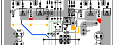
The traces for rails and about parts of the traces to the output devices are much narrower than the rest of these traces in the R24 and R27 areas that feed R29 - R32.
[snip]
Regards,
John L. Males
Willowdale, Ontario
Canada
08 July 2007 13:16
Official Quasi Thread Researcher
jethari said:
John
[snip]
The feed traces to R29-R32 need not be that heavy IMHO as the trace lengths are pretty short. Very heavy traces are required over long lengths to offset possible current loss. All the same, I've increased the trace width marginally.
[snip]
Thanks
Hari
jethari said:Hi all
I finally managed to create the pdf file of my pcb layout (nmos350) in under 100Kb size. Please do go through this with a tooth comb and give me your feedback.
John (keypunch), thanks a million for your tips on creating a smaller pdf file. I have also incorporated the changes that you suggested in the layout.
Hari
Hi Hari,
I think I was not clear enough in my comment re the trace being too thin comment I made, which was for the high current part of the trace I was referring to in my above comment. To enable things to be clearer on that point with a proposed solution and some other points since my last comments I have created a .PNG image with colour coding to hopefully improve the clarity of my comments.
1) With respect to the "traces for rails and about parts of the traces to the output devices are much narrower than the rest of these traces in the R24 and R27 areas that feed R29 - R32" I was referring to the trace area in the attached image marked in red. This is the narow rail trace I was making reference to. A proposed solution I have since I first pointed out is marked partly in orange. I would remove the trace that connects R20 to R24 and R23 currently. I would then add the orange trace to the effect I have below R20/R23/R24 and connect R20/R24/R23 across the wide trace and then fill in the narrow trace that R24 causes to the same wide trace. I would effect as similar change on the R22/R26/R27 side which I have only partly marked in in orange as it would take me too much time to move things about with the GIMP editor. First you would need to lower L1 to make room for the a trace like I proposed for R20/R24/R23 in orange so you could effect a similar replacement trace for R22/R26/R27 and remove the existing trace that connects R22/R26/R27. Then you could fill in the narow trace caused by R27 to the same wide trace width while R26/R27 connect over the thick trace.
2) Right now you have the R17 to R35 NFB connection trace going via R29/R31/R20. This could create curent loops on the V+ output side of the signal and general practice is to ensure the NFB point is directly connected with the output point of the Zobel Network, in this case the R35 point. I would remove the trace from R17 to R29 and run an insulated under the board wire connecting R35 to R17. If you wish to make a solder hole in the wide trace near R35 for this insulated wire link I am sure that will be just fine.
I trust the more descriptive explaination and the attached colour coded image will enable my thoughts to be clearer.
Regards,
John L. Males
Willowdale, Ontario
Canada
12 July 2007 (22:00 - 01:00)
14 July 2007 (11:50 -) 12:48
Official Quasi Thread Researcher
Attachments
jethari said:Whew! I think John's just broken his own record!! Jokes apart, that's one of the best explanations about power requirements that I've ever come across. He's put the whole thing about power into the correct perspective. Great!!!
Hari
p.s. John, still waiting for your clarifications on my pcb layout.
Hi Hari,
LOL LO LOL LOL
Thanks for your compliment. I am sure there are other opinions on power requirements out there. I can think of the Class A fans for one. Anyway, this is my take, research, real world measurement and take on power requirements. I have no clue what the sensitivity of my speakers are, but I suspect they are about 83dB - 85dB and passive crossover based. I had a 50W RMS amplifier for many years that had VU Meters, not LEDs on it, so I know all to well what the power demands have been for average and moderately high levels into a passive 3 way speaker system. One of my quasi amps elements will be to have a RMS and Peak meter on it. Likely LED and will be at least 20 step LED in 3 dB steps and two settings, low and high range scale. The 5 channel amp I have now has no metering on it 🙁 With an active crossover removing the passive crossover I would guess the amps that would power them would only need about 0.25VRMS average listening and 4VRMS peak. I will know better once I have at least 6 quasi amps built and of course a 3 way active crossover. 😉
I was working on the image attachement and review of PCB Thursday evening when arrived home a bit earlier. Some more on the image after the prior posting I did not expect to take me so long to type in and review for typo errors. I only saw your wish for my PCB comments after I actually posted my comments with the PCB image to help with the explaination.
I am sure there will be other comments to follow about my PCB suggestions by the thread.
Regards,
John L. Males
Willowdale, Ontario
Canada
14 July 2007 (12:50 -) 13:05
Official Quasi Thread Researcher
- Home
- Amplifiers
- Solid State
- Power amp under development