Hari's Latest Version of the NMOS250 PCB
Hari,
Sadly my browser crashed as I was reviewing and correcting my typing of my reply of this morning and all my comments were lost about your latest PCB version. I had some things to do so I am sorry for the delayed posting of my comments re nmos composite 2607.pdf of Post #2120:
1) In your second last PCB image, nmos circ coil.pdf, of Post #2082 you had a PCB change to for a "pcb with a more toroidal coil for L1". However in your latest PCB of Post #2120 the change for "more toroidal coil for L1" is not reflected. Did you decided to return to the more traditional way of winding and positioning L1?
2) Currently C5 and C6 bypass the front end at the end of the front end with respect to +-Vrail rather than I believe should be the start of the front end with respect to +-Vrail. I know how you have C5 and C6 located and traced currently and thus far is the same as how quasi has his TO-247 NMOS200 PCB designed. The "classic PCB" does have the same location for C5 and C6 physically, however because the +-Vrail are connected and trace from the output MOSFET exectrically C5 and C6 are bypassing the +-Vrail before the rail supplies the front end. To configure your PCB in the same electrical sense as the "classic PCB" I would move C5 so that C5 connects between the V POS/R4 node and the C11-/C9 node at C9 via a trace. It may be necessary to shorten the short leg of the V POS wide trace "L" of the by moving the V POS pad to the PSU and F1 to the left to accomodate any extra space C5 or related trace to the C11-/C9 node trace. Likewise for C6 to be moved so that C6 connects to the V NEG/R7 node and then a trace to the C13+/C10 node. I think the "experts" will be able to comment further to the rational for moving C5 and C6.
3) That said for (2) maybe, and it is just a thought that occurred to me, you just add a C5A and C6A at the front end as well and leave the current C5 and C6 where they are. I suspect the "experts" will be able to comment if there is any merit to this suggestion. My sense is there would be no merit, but seeing as the thought just crossed my mind I thought I would present the idea in case there is some merit to the idea or refining comments by the "experts".
4) T8 should be centered between T9 and T10 for thermal considerations.
5) The traces for C11+ and C13- should be wider. There is no need to move C11 or C13. All one would do is shave off the wider than rest of the V POS and V NEG rails traces on the inside sides of the of the PCB traces on the side and add it to the existing C11+ and C13- traces returning to the respective +- Vrail they are currently connected to.
If and when you wish to add the option for the Leach Feedforward NFB (overview of Leach design) let me know. I can guide you what extra links, pads and such to accomodate the extra 3 parts to allow builders to choose to use the Leach Feedforward NFB option of with the quasi NMOS design.
Regards,
John L. Males
Willowdale, Ontario
Canada
29 July 2007 (10:30 -) 11:45
29 July 2007 (14:13 -) 15:59
Official Quasi Thread Researcher
Hi John
Thanks once more for your observations.
1) Yes I decided to stick to the more conventional coil design. Using some popularly available inductor calculators I found that there is not much difference between the two types especially for this value. That said, I still have the circular coil design saved for anyone who is interested.
2) The location of C5 and C6 is exactly the way Quasi has used it in his nmos200 pcb layouts. Remember the basic building block for my design was Quasi's nmos200 design.
3) Same as 2)
4) I've shifted T8 so as to be centered between T9 and T10.
5) Again, if you look at Quasi's design for the nmos200, he has used separate traces for C11 and C13 to prevent a high current surge going through the caps. Quasi's comments are there on one of the posts in reply to my original pcb design.
Cheers
Hari
Hi,
the caps C11 & C13 send pulses into the ground connections.
Those pulses run between the two connections and generate a voltage between the two connections if they are not coincident.
Either move the ground links so that they share the same spot at the corner of the power ground,
or
join the two cap grounds together and run a short link to the power ground.
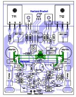
G,day Hari,
This picture illustrates one of the points AndrewT made. All power supply bypass capacitors have their own exclusive track to a central ground on the board. I have coloured the relevant tracks and links in green. The 0.1uf caps in parallel with the electrolytics share a track, but this is ok because they are essentially one capacitor.
This grounding methodology is important in order to achive low levels of noise and distortion.
Cheers
Q
Attachments
quasi said:G,day Hari,
This picture illustrates one of the points AndrewT made. All power supply bypass capacitors have their own exclusive track to a central ground on the board. I have coloured the relevant tracks and links in green. The 0.1uf caps in parallel with the electrolytics share a track, but this is ok because they are essentially one capacitor.
This grounding methodology is important in order to achive low levels of noise and distortion.
Cheers
Q
Quasi
I would have thought that providing large areas of copper "land" would eliminate the possibility of any voltage building up across ground connections.
Hari
Hi Hari,
The charge and discharge currents can be quite large and even a tiny amount of resistance can create a tiny difference in voltage. In the case of your board you have the 0.1uF bypass capacitor on the tracks feeding the input stage sharing a ground path with the capacitors on the output stage rail. Now the track between their connections is short and wide but there could be an amp or more of charge and discharge creating just a few millivolts on the supply feeding the input stage. This may not be heard at low volume, but it will affect the ability for the amp to be low in distortion.
Maybe this level of design is too picky for some people, but the correction is too simple to neglect.
Cheers
Q
Quasiquasi said:Hi Hari,
The charge and discharge currents can be quite large and even a tiny amount of resistance can create a tiny difference in voltage. In the case of your board you have the 0.1uF bypass capacitor on the tracks feeding the input stage sharing a ground path with the capacitors on the output stage rail. Now the track between their connections is short and wide but there could be an amp or more of charge and discharge creating just a few millivolts on the supply feeding the input stage. This may not be heard at low volume, but it will affect the ability for the amp to be low in distortion.
Maybe this level of design is too picky for some people, but the correction is too simple to neglect.
Cheers
Q
Got your point. I've made the changes. Here is the updated layout.
Hari
Attachments
Hari,
What version of Protel are you using for your PCB?
Regards,
John L. Males
Willowdale, Ontario
Canada
30 July 2007 22:05
Official Quasi Thread Researcher
What version of Protel are you using for your PCB?
Regards,
John L. Males
Willowdale, Ontario
Canada
30 July 2007 22:05
Official Quasi Thread Researcher
keypunch said:Hari,
What version of Protel are you using for your PCB?
Regards,
John L. Males
Willowdale, Ontario
Canada
30 July 2007 22:05
Official Quasi Thread Researcher
John
I'm using Protel DXP version 7.0.737
Hari
anybody fully assembled the amplifier & tested it?
Waiting 4 their results & final layout, schematics.
Waiting 4 their results & final layout, schematics.
Hi jaya000,
All about Quasi's designs you can found here:
http://www.adam.com.au/cgpap/QuasiWeb/index.htm
Regards
All about Quasi's designs you can found here:
http://www.adam.com.au/cgpap/QuasiWeb/index.htm
Regards
Hari, how much power will your version put out?
Also, I was thinking how it would work out if I used 2N3055 (100V, 15A, 115W) transistors for the bipolar version initially. I have a lot of them lying around at home. I also have a 25-0-25 V 12A transformer. How would that work out?
Also, I was thinking how it would work out if I used 2N3055 (100V, 15A, 115W) transistors for the bipolar version initially. I have a lot of them lying around at home. I also have a 25-0-25 V 12A transformer. How would that work out?
Vivek said:Hari, how much power will your version put out?
Also, I was thinking how it would work out if I used 2N3055 (100V, 15A, 115W) transistors for the bipolar version initially. I have a lot of them lying around at home. I also have a 25-0-25 V 12A transformer. How would that work out?
Vivek
Ther version I'm planning would be about 160W rms per channel into 8 ohms.
I've attached a comparision chart for the two types of transistors.
With a 25-0-25 transformer you'll barely get 50W for which you'll not need as many pairs as shown in Quasi's schematic.
cheers
Hari
Attachments
That transformer probably has multiple secondary windings. All the tappings are probably soldered together inside the insulation and brought out as single large area flexible leads.Vivek said:I also have a 25-0-25 V 12A transformer. How would that work out?
Is this a toroid?
Are you prepared to do some work?
I had a 500VA 25-0, + 25-0Vac and internally it had three bifilar wound secondaries. I split them up, added a fourth and got 25-0,+25-0,+25-0,+25-0Vac If you could do something similar you have the choice of four 25Vac windings or two 50Vac windings.
The four windings could be used for a 200W +200W into 2ohm amp (pretty useless) or a 400W into 4ohm. That sounds like an animal, if you need/can use that high a power level.
Hari, I will take a look at the comparison chart.
Andrew, So I will have to rip open the transformer and check, right? I don't mind a little dissection anyway.
But what about the use of 2N3055 output transistor?
Andrew, So I will have to rip open the transformer and check, right? I don't mind a little dissection anyway.
But what about the use of 2N3055 output transistor?
Hi V,
no, don't rip open.
Open it carefully and keep the insulaton in good condition, you will need it to re-wrap the secondaries when you're done.
The kapton/mylar tape is not easy to source in small quantities.
You should not need to unwind the secondary, it will become obvious how it's been assembled when you get some/all of the outer insulation off.
If you need to add a winding to make it symmetrical, just measure the existing solid core wire and buy enamelled copper to match. It's usually sold in 500g reels.
The one I have is an EI transformer. There is a wrapping on the winding which looks like thick card paper. I am not sure what the material is. Anyway, there is a thick layer of varnish on the winding. It is going to be a problem to get that out first.
And what about my idea about using 2N3055 transistors because they are cheap. I dont mind a little less power. In the chart, collector current is almost the same. Icc and Vceo are much higher in the 2N3733.
And what about my idea about using 2N3055 transistors because they are cheap. I dont mind a little less power. In the chart, collector current is almost the same. Icc and Vceo are much higher in the 2N3733.
EI!
you won't have much room for an extra winding.
How do you avoid damaging the insulating oxide on the laminations if you take it apart?
you won't have much room for an extra winding.
How do you avoid damaging the insulating oxide on the laminations if you take it apart?
- Home
- Amplifiers
- Solid State
- Power amp under development