Hello...
I have worked arround a bit with an amplifer design..
Its based arround a J-fet input . that is a little unconventional coupled as a little of the signal is fed to the corrent source for the second stage..
The amplifer simulates wery well with very low distortion and a quite unique distortion distribution as the second harmonic dominates by a factor 10 to the third...
All in all a rather promising design..
I have som questions regarding the output stage...
Would it be possible to omit the predrivers as I already have rather powerful transisters arround the bias spreading diode string.. and the drive the drivers directly..?
I have made a DC-coupled feedback is this desireable or must I insert DC-blocking... ??
if so I have to raise impedance in the feedback loop by app. a factor 5
Attachments
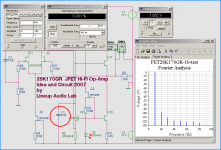
DC component:-0.00176547
Harmonic Frequency Fourier Normalized Phase Normalized
Number [Hz] Component Component [degree] Phase [deg]
1 1.000e+03 8.162e+00 1.000e+00 180.00° 0.00°
2 2.000e+03 3.483e-04 4.268e-05 90.14° -89.85°
3 3.000e+03 2.063e-05 2.528e-06 -177.61° -357.61°
4 4.000e+03 5.119e-07 6.272e-08 -107.15° -287.14°
5 5.000e+03 1.872e-07 2.293e-08 -179.65° -359.64°
6 6.000e+03 2.682e-07 3.287e-08 176.29° -3.71°
7 7.000e+03 3.419e-07 4.189e-08 179.23° -0.77°
8 8.000e+03 3.360e-07 4.117e-08 -178.04° -358.04°
9 9.000e+03 3.677e-07 4.505e-08 179.32° -0.68°
Total Harmonic Distortion: 0.004275%
Attachments
MIIB
Nice design,
It looks like a combination of Hafler Transnova circuit along with Folded Cascode loaded VAS.😉
Nice design,
It looks like a combination of Hafler Transnova circuit along with Folded Cascode loaded VAS.😉
Yes, you should be able to remove one driver stage.
I think the test results would not be so much bad.
I would start with try this:
- Remove Q13, Q11
- Replace Q18, Q19 with MJE15030, MJE15031
DC-Coupled feedback. Quite alright!
When we have JFET pair as input, we have almost no input bias current.
When using BJT, it is these very small currents, that create a different voltage drop
across feedback resistors(R45//R2) vs. Input resistor (R9).
Say we have a bipolar input pair. Into BASE of each transistor runs 1 uA.
R9 = 47000 ohm = voltage across R9 = 47000 x 0.000001 uA = 47 milliVolt
R45 // R2, paralleled 2000//50 gives combined resistance = 48.78 Ohm
Voltage across this resistance = 49 Ohm x 1 uA = 0.049 mV
The differential input pair will amplify (x40) the difference:
40 x [0.047 V - 0.000049 V] = 1.878 Volt DC-Offset at output.
With a blocking capacitor for R2 (50 Ohm) the resistance difference (for DC-current) would be 47 kohm vs. 2 kohm, which is smaller, but still too much (45000 ohm x 1 uA).
But if you would use R45 = 47 kohm, there would be no difference for the resistance bias current would see, and very little voltage difference at BASES of input pair.
And so not much DC-offset at output.
---------------
When using JFET input pair we have almost no input bias current.
And so we get no voltage drop across bias resistors, and no offset from this.
But we can get offset because the JFET input pair has different Volt Gate-Source.
So we may have to run these two FET with different current in each transistor. We balance current so that Vgs will be equal = no offset.
I see you may have used R4 for this current balancing in the input pair.
With real JFETs you may have to make R3(270ohm) and R4(262.4ohm) even more different.
Lineup, I think one could rather remove Q6 and Q7. The output is a cfp driver EF, its one of the best output stages performance wise. Big improvementt on standard EF. It has very high input impedance and I think it could be driven by Q4 and Q5 alone.
I did something similar a while back, just cant find my sims between all the thousands of files I have, which yielded quite good performance. Ill try and find it. By similation one could tell which works best.
I did something similar a while back, just cant find my sims between all the thousands of files I have, which yielded quite good performance. Ill try and find it. By similation one could tell which works best.
Yes, homemodder
Removing Q6 and Q7 is an option to try out.
Of course the ~ 1 mA from Q4 and Q5 may be a bit too small for the need of the diode string. (input pair 3 mA/each)
Currently there is ~12 mA through diodes. Set by CCS transistor Q7.
Trying my option first, would not change anything for conditions of the Bias setting diodes.
Another thing is some Stability Compensation capacitance.
If you find that you need this, one way to try is to add C1 like in my JFET Hifi Opamp.
This same way is used in Hi-Fi op-amp AD797.
( Topic: New JFET Hifi Op-Amp - by lineup )
The value needed to ensure good stability may be in the range: 22pF - 220pF
See attachment = C1
Attachments
Lineup
thanks for the advice om the outputstage...
I'll try to manke both version in my sims,,. i already did your first suggestion.. Turned out quite good.. But still i have a hunch that it won't sound as solid as the version with predrivers..
Also thanks for the hint on HF-compensation.. nice way to implement it..
michael
Hi Michael. Unusual design. Would you elaborate on your choices?
Test. Without referring to your simulation, what do you think determines the feedback loop's unity gain frequency?
Brian
Test. Without referring to your simulation, what do you think determines the feedback loop's unity gain frequency?
Brian
This is basically en elboration on the Ad opamp discribed by lineup..but with differnt transistors and differetn current sources..
I saw that the design holds a unique dirtortion distribution alongwith the fact that i was possible to put cascodes so it could scale and grow into a poweramp..
I have built one with linear mosfets in the output... it had the most natural mids and high, but lacked the absolute punch in the base... as with most mosfet designs...
So now its fittet with a bipolar output design. Hope this will add the extra dimension.. and bottom end drive that is a must..!
I have decided to try to remove the output buffer on the voltage amplifer and then integratre the diode bias spreader into the second summing stage...
I'll then have to change the transistors into a more ressiliant type and ajust so that more current is available through the diodestring.
This is possible due to the high input impedance of the outputstage
I'll return with schematics and sim results...
I'll then have to change the transistors into a more ressiliant type and ajust so that more current is available through the diodestring.
This is possible due to the high input impedance of the outputstage
I'll return with schematics and sim results...
Hi
That's my output stage! 😀
R44 should be around 1ohm, not 0.1ohm. With actual value, the CFP driver will ring at high power levels.
Nice design!
Mihai
That's my output stage! 😀
R44 should be around 1ohm, not 0.1ohm. With actual value, the CFP driver will ring at high power levels.
Nice design!
Mihai
Redesign input cascode.
At startup C4 is discharged and jfets will experience full supply voltage. Also the PSRR will not be very good, especially when input with power supply ripple intermodulation is concerned.
Current source instead of R19 and C4 will be much better.
Regards
Adam
At startup C4 is discharged and jfets will experience full supply voltage. Also the PSRR will not be very good, especially when input with power supply ripple intermodulation is concerned.
Current source instead of R19 and C4 will be much better.
Regards
Adam
Dark frienz
I take that your suggestion for the casodes is a currentsource with resistor devision and then referenced to gnd...
I thought about it but was a little afraid off dirty gnd..
That was my motivation to make it this way..
I can see your point i frying the J-fets at start-up may not be the best of ideas
Thank for comments
I'll post revised schematis start of next week'
I understand the idea of attaching cascode bias resistor to same curerrent souurce as input pair.
You want the cascode to follow the input voltage.
But I am not sure this is good. The cascoding bias current may upset the input.
Normal cascoding will attach only at supply lines.
Using at least V+ V-.
And sometimes also GROUND level to set the voltage of cascode.
You want the cascode to follow the input voltage.
But I am not sure this is good. The cascoding bias current may upset the input.
Normal cascoding will attach only at supply lines.
Using at least V+ V-.
And sometimes also GROUND level to set the voltage of cascode.
Referencing to the "long tail" is perfectly fine, you just mustn't upset the constant current as lineup pointed.
darkfenriz said:Referencing to the "long tail" is perfectly fine, you just mustn't upset the constant current as lineup pointed.
Hi Lineup and darkfenriz
Can you please elaborate ... what do you mean with "upset the LTP CCS"?
what i mean is, the cascode resistors will inject current variations into the LTP pair
as the voltage across these resistors will vary along with input voltage
if the casode bias is done with a ccs from V+,
then of course the current into LTP pair will be constant
i have no experience of this type of input following cascode
so I do not know if it has got any substancial benefits
compared to ordinary cascoding refering to supply lines only
lineup said:what i mean is, the cascode resistors will inject current variations into the LTP pair
as the voltage across these resistors will vary along with input voltage
if the casode bias is done with a ccs from V+,
then of course the current into LTP pair will be constant
i have no experience of this type of input following cascode
so I do not know if it has got any substancial benefits
compared to ordinary cascoding refering to supply lines only
In the first case, the LTP common mode will reject all the garbage induced by the voltage variation over the cascode biasing resistor. The only thing we must worry is the percent of current needed for cascoding compared with LTP current.
The second case, with a CCS from positive rail biasing the cascoding resistor, is frequently used in many commercial design. In my design, RMI-FC100, I used with success this type of cascoding method.
http://www.diyaudio.com/forums/attachment.php?s=&postid=1349109&stamp=1194852081
In order to balance this design the cascode voltage mus be half of the supply voltage..
If we the see supply ripple and we use a constant current source to fix the voltage at ex 27 V.. we would see the psu ripple also at the out put..
Mihai
I like the led loadede CCS but i must sim some more to see if its possible to use in this dessign..
Thanks for the inspiration along the output-stage--- I have great respect for the work you have made to use the diode compensation and to finde the right level of that.
MiiB said:In order to balance this design the cascode voltage mus be half of the supply voltage..
Don't use more than 10V Vds for 2sk170 😉
What do you know about fet gate leakage ?
- Status
- Not open for further replies.
- Home
- Amplifiers
- Solid State
- Power Amp Design