Thanks
I'll balance it out with a cascode placed at +10-12 V...!
This will also reduce thermal stress on the input fets
michael
I'll balance it out with a cascode placed at +10-12 V...!
This will also reduce thermal stress on the input fets
michael
watch out for C6!
Miib,
Assuming the schematic hasn't changed, C6's location could cause problems. At turn on, it would force a lot of current through Q17, and might destroy Q8. Further, in that position it harms the PSRR of the current source. Perhaps you could improve the topology by splitting R12 into two 5K pieces, and moving C6's connections to the junction of the two 5Ks and the negative rail.
I cannot see V4 and V5 values on schematic, so I assume 48V in the rest of my post
(maybe something wrong with my PDF viewer).
C6 is obviously in wrong place. It should be connected to negative rail, not to ground. Also C4 semms to not make sense at all. With such connection the resistance seemed from Q8 collector is 5k, which makes using current source not needed. Instead Q8, 7.3k resistor will make the same effect, and PSRR will be only little worse. And another thing - Q8 current is about 6.5mA, and R18,R19 takes 4.8mA, so very little rest for four JFET's.
So mys suggestions:
1. Replace that C6 as suggested in previous post.
2. Replace R19 with current source about 1-2mA - as in Roender design.
3. Repalce R18 with zener pararelled with 1u capacitor.
You get amazing results with simulation at 1kHz, but I'am more interested at 20kHz - thats
always differrent and more interesting. Im also curious about Your simulation models.
In LTSpice some model found on the net gets very strange results, when amplifier is
overdriven (even at 1kHz) - can You try this?
Anyway - very nice and interesting design - Im gonna try some like this in future
(that input stage)...
One interesting thing: on many posts on this forum people says that in JFET input
stage, current source and source-followed cascode is the best option. That is
the way of Roender design, and many other, also commercial amps.
But there may bo another way - something like this design - no CCS and resistance
loaded drain, which make them less linear, but sounds better, I mean better harmonics
distribution, higher second, lover third and so on.
wojtek5001 said:
...
3. Repalce R18 with zener pararelled with 1u capacitor.
...
I would not do that. You don't need a low impedance in base of a common base circuits, it can oscillate like hell.
CCS from positive power supply and a resistor would be enough ... and maybe a 1n4148 diode in series with resistor for cascode thermal tracking
O.K., if it can oscilate, ther better not use capacitor, also Zener diode might be noisy
without it, so resistor might be better. But use diode for cascode thermal tracking will be little overkill in my opinion.
without it, so resistor might be better. But use diode for cascode thermal tracking will be little overkill
in my opinion.memory distortion thermal compensater cascode....??
Maby it could be fun to try a superregulated frontend supply and the loose all current sources...!
just a thought
Maby it could be fun to try a superregulated frontend supply and the loose all current sources...!
just a thought
Worked a bit more with the desig...
Changed cascode to a TL432 based current source referenced to GND
Further suggestions welcome to this issue...!
Inproved input current stage
Removed inputstage buffer stage to drive output directly..
When overdrived the amplier clips nice an symetrically.
open loop bandwith is app 20 KHz with 78 dB gain
closed loop is app 1 MHz at 33 dB gain
Attachments
Distortion figures remain low
increases to app 5 time this value to o.o2 when driven hard close to clipping .
increases to app 5 times to o.o2 at 20 Khz 0.2 V in.
The ditribution remains the same eg mainly second than lover third.. then almost none.
Fourier components of V(out)
DC component:-0.000663182
Harmonic Frequency Fourier Normalized Phase Normalized
Number [Hz] Component Component [degree] Phase [deg]
1 1.000e+03 8.159e+00 1.000e+00 179.98° 0.00°
2 2.000e+03 3.892e-04 4.770e-05 86.47° -93.51°
3 3.000e+03 1.942e-04 2.381e-05 10.30° -169.69°
4 4.000e+03 3.488e-06 4.275e-07 90.23° -89.75°
5 5.000e+03 1.124e-04 1.378e-05 17.22° -162.76°
6 6.000e+03 1.578e-06 1.934e-07 94.00° -85.98°
7 7.000e+03 7.212e-05 8.840e-06 24.54° -155.44°
8 8.000e+03 8.942e-07 1.096e-07 98.40° -81.58°
9 9.000e+03 5.185e-05 6.355e-06 32.02° -147.97°
Total Harmonic Distortion: 0.005613%
Led based CCS loeded casoded with thermal tracking
Jfets now running at 12 V vith 1.5 mA throug each...
Maybe they should run with higher current..?
This would mean channge of CCS transistors to acommedate higher current or to remove one set of the jfets.
michael
Jfets now running at 12 V vith 1.5 mA throug each...
Maybe they should run with higher current..?
This would mean channge of CCS transistors to acommedate higher current or to remove one set of the jfets.
michael
Attachments
What is the max IDSS of some real 2SK369?
I would run them high. Like 50-75 % of max, maybe more if possible.
Higher current will increase the gain.
And in this amplifier those JFETs are providing all the gain to the follower part.
You will need all the gain you can get from this input
I would run them high. Like 50-75 % of max, maybe more if possible.
Higher current will increase the gain.
And in this amplifier those JFETs are providing all the gain to the follower part.
You will need all the gain you can get from this input
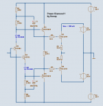
Here is another output stage.
Power Diamond
Uses 2 driver stages + Output, just like in your Follower.
By adjusting R1, R2, R8, R9 we can set the idle bias like 50-100 mA.
D1, D2 should be placed in contact with main heatsink, for thermal tracking.
MJE15028, MJE15029 drivers should have separate heatsink.
With the bootstrapping C1, C2 capacitors
and the regulated +-28 Volt supply for driver stages,
this output has very low distortion.
Attachments
MiiB said:Worked a bit more with the desig...
Changed cascode to a TL432 based current source referenced to GND
Further suggestions welcome to this issue...!
Inproved input current stage
Removed inputstage buffer stage to drive output directly..
When overdrived the amplier clips nice an symetrically.
open loop bandwith is app 20 KHz with 78 dB gain
closed loop is app 1 MHz at 33 dB gain
More than 40dB at 20kHz with single-pole compenstaion means certain oscillation problem. You could squeeze around 60dB of problem-free feedback using two-pole, but 78dB is way of the range.
Your amplifier roll-off OLG only with the help of internal parasitic capacitance ... not good IMHO.
Any folded cascode stage need some sort of load to ground (lag) compensation
Any folded cascode stage need some sort of load to ground (lag) compensation
added hf 47 pF stabelising cap. this reduces OLG bandwith to 8KHz .
now phaseshift looks more promesing and stays withing 90 degress going towards 100 mHz - I take that this will add to stability of the design.
Increased current to 6 mA through Jfet's
Getting closer
now phaseshift looks more promesing and stays withing 90 degress going towards 100 mHz - I take that this will add to stability of the design.
Increased current to 6 mA through Jfet's
Getting closer
Attachments
I have now started the PCB artwork..
Ill try to make a star on star gnd with a wire conecting the PWR GND to signal gnd..
I belive this is a good staregy.. i have previously tried to make PCB with ground and power planes, but i didn't mangage to get it right..
I'll post as i get along..
thanks for input this far..
michael
Ill try to make a star on star gnd with a wire conecting the PWR GND to signal gnd..
I belive this is a good staregy.. i have previously tried to make PCB with ground and power planes, but i didn't mangage to get it right..
I'll post as i get along..
thanks for input this far..
michael
- Status
- Not open for further replies.
- Home
- Amplifiers
- Solid State
- Power Amp Design