Even if I raised a similar question in the Chip Amps section, and headphone amps looks like a VERY large field, perhaps someone can tell me a story on what made a remarkably good audio for them.
My requirements are:
1) 12 single supply.
2) Must drive 50-75 ohm headphones to good levels, 600ohms if possible. So capable of large current.
3) Using output boost is an option.
4) It must use chips, not transistors or valves.
My requirements are:
1) 12 single supply.
2) Must drive 50-75 ohm headphones to good levels, 600ohms if possible. So capable of large current.
3) Using output boost is an option.
4) It must use chips, not transistors or valves.
I made something like you are looking for a while ago. Although I made an emphasize on lover idle current, as it was going to be powered from a 9V battery. Should be no problem running it on 12V. Here how it looks like:

If you are interested, I can try to dig up the schematic.
Also I would like to point to some miss-concept in your requirements. If you willing to drive ~600Ohm load, you will need higher voltage, but not currents swing. In this case single 12V might be a limiting factor, unless you will add an SMPS or charge pump to boost or invert supply voltage.
Yes, please try to dig up your circuit. I'm very curious.
And yes, it should be unlikely I will be able to get anything from 600ohm loads.
And no, no SMPS for anything on this project. There will be 48v supply for the microphones, but very low current.
And yes, it should be unlikely I will be able to get anything from 600ohm loads.
And no, no SMPS for anything on this project. There will be 48v supply for the microphones, but very low current.
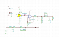
The amplifier itself look pretty much like this. I've simplified it a little bit. There where a few extra things which I think will not make too much difference.
There is also a supply rail splitter on that board, based on LM7322. It generates mid supply of 9V. This mid supply also was used as a signal ground. Depending on supply arrangement in your case, it may not be possible to reuse such solution.
Also, if supply source allows, some different opamp may be chosen for the design. These low power high speed guys are quite touchy in terms of stray capacitance.
Attachments
Hi Sergey,
Your design is based on Walt Jung's composite opamp design, which might have some restrictions for me, as my supply is 12v analog, as I said.
I do have to create a V+/2 reference ground, so I don't see how I could apply it to that circuit, if at all possible.
Your design is based on Walt Jung's composite opamp design, which might have some restrictions for me, as my supply is 12v analog, as I said.
I do have to create a V+/2 reference ground, so I don't see how I could apply it to that circuit, if at all possible.
This design is perfectly usable with unipolar +12V supply with a half supply "virtual ground". You just need to change net names as per what you have on your board. +V goes to +12V, -V goes to 0 and ground goes to you virtual ground - 12V/2.
Depending on how you are going to organize virtual ground, you may need if add DC decoupling capacitors. Although it is better if you can avoid to have one. At least at the output path.
Yes, DC decoupling capacitors are needed in V+/2 arrangements. But that is not such a serious problem to me.
But two questions are on that design:
1) If I can replace the global feedback resistor with a pot, to set levels, as I can't use a pot a the input.
2) How to connect Vref in the inside chip.
It's not that easy to replace the grounds connections with Vref. Some you can't.
But two questions are on that design:
1) If I can replace the global feedback resistor with a pot, to set levels, as I can't use a pot a the input.
2) How to connect Vref in the inside chip.
It's not that easy to replace the grounds connections with Vref. Some you can't.
I like multiloop composite amps with CFA output - but sergey's circuit, gain/feedback values may push stability limits
I really wouldn't try that without a local feedback C on the input op amp to slow the global loop - with the LMH6723 at Av 11 you are dropping to a few 10s to MHz corner (CFA do run out of GBW at high gains), may add too much phase shift for the 22 MHz input op amp
wanting 100+ mA output and portable aren't a good combo for battery life
the OP should clarify his "12 V" supply details - the LMH6723 abs max 13.5 Vs may be exceeded if ever ran from a unregulated "12 VDC" wall wart with poor the regulation of a small xfmr being pushed to limits for cost
likewise some battery type nominal and peak fully charged V differ by enough to matter in chip choice
the AD8397 is a possible choice for the output current - but handling the power dissipation from its tiny power pad may be a challenge - the tiny pad is harder to solder by hand
I've used the TPA6120 - still surface mount, power pad - but much bigger - Peranders project pages shows it being soldered by hand
Last edited:
Well, the supply would never be unregulated wall wart, as it will always be battery powered.
There might be an external DC input, but it would be regulated inside.
Though I would prefer chips that can take up to 18v at least, because batteries may be 14.2v sometimes. We are still considering if we regulate to 12v or not.
The design I'm favoring for now is an NJM4556 with transistor boosting at the output. I'm looking for options that can improve on that, but they should be simple to implement and not expensive.
2 jcx
If you have a look at feedback divider values and components, you may notice that loop 0dB frequency is actually not too high, around 9MHz, and the phase margin is rather generous, as per simulation. It may be reasonable to move it lower, for better repeatability, but there is nothing like you say tens of MHz.
If you have a look at feedback divider values and components, you may notice that loop 0dB frequency is actually not too high, around 9MHz, and the phase margin is rather generous, as per simulation. It may be reasonable to move it lower, for better repeatability, but there is nothing like you say tens of MHz.
Last edited:
Yes, DC decoupling capacitors are needed in V+/2 arrangements. But that is not such a serious problem to me.
But two questions are on that design:
1) If I can replace the global feedback resistor with a pot, to set levels, as I can't use a pot a the input.
2) How to connect Vref in the inside chip.
It's not that easy to replace the grounds connections with Vref. Some you can't.
1) Not in this case
2) In general, all small signal connections go to you Vref. With the load connection you may do several different ways. If mid supply generator has sufficient driving capabilities, load can be connected to it. If not - it can be connected through a decoupling cap to your real ground.
Also you must be careful there, as you may inject you reference signal noise into your signal chain. You need to be more specific about what you are doing if you want to get a good answer. Some sketch may really help.
wanting 100+ mA output and portable aren't a good combo for battery life
the AD8397 is a possible choice for the output current - but handling the power dissipation from its tiny power pad may be a challenge - the tiny pad is harder to solder by hand
I've used the TPA6120 - still surface mount, power pad - but much bigger - Peranders project pages shows it being soldered by hand
Nothing in this project will be soldered by hand. It is not a DIY project.
If I can't set the levels in the feedback, then I can't use the composite.
The point I will be picking the signal from does not allow putting a level pot.
the OP should clarify his "12 V" supply details - the LMH6723 abs max 13.5 Vs may be exceeded if ever ran from a unregulated "12 VDC" wall wart with poor the regulation of a small xfmr being pushed to limits for cost
likewise some battery type nominal and peak fully charged V differ by enough to matter in chip choice
Was about to ask the same question, as for example car battery "12V" will be a bit of a problem for this chip.
2 carlmart
It is possible to make a composite where pot can be used in a feedback loop, but I do not see such arrangement optimal. Will it be better to add intermediate stage using one more low power opamp? Actually, what is you power consumption requirements?
It is possible to make a composite where pot can be used in a feedback loop, but I do not see such arrangement optimal. Will it be better to add intermediate stage using one more low power opamp? Actually, what is you power consumption requirements?
if you want a fully debugged example you might look at The Mini³ Portable Stereo Headphone Amplifier
and of course the O2 project - which as a thread here too
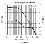
Sergey - see figure 17 in the LMH6723 datasheet - you really don't want to stack poles that close in frequency inside the global loop
I like to see >~3:1 separation of pole frequencies for a fast buffer/current gain stage inside the global loop and the gain intercept - for your values you need to slow the loop, or rearrange the gains
for instance dropping the gain of the LMH6723 to less than the global loop gain (or the high frequency "noise gain") setting is valuable - say to +5
I would like to see your gain and phase margin plots from sim, and if the chip models response agree with the datasheet specs for the chips
and of course the O2 project - which as a thread here too
Sergey - see figure 17 in the LMH6723 datasheet - you really don't want to stack poles that close in frequency inside the global loop
I like to see >~3:1 separation of pole frequencies for a fast buffer/current gain stage inside the global loop and the gain intercept - for your values you need to slow the loop, or rearrange the gains
for instance dropping the gain of the LMH6723 to less than the global loop gain (or the high frequency "noise gain") setting is valuable - say to +5
I would like to see your gain and phase margin plots from sim, and if the chip models response agree with the datasheet specs for the chips
Last edited:
2 jcx
Seems like you are missing presence of R2 C3 chain.
Also, did you notice that LMH6723 is actually a CFA?
LMH6723 model is not perfect, but not too bad as well.
Seems like you are missing presence of R2 C3 chain.
Also, did you notice that LMH6723 is actually a CFA?
LMH6723 model is not perfect, but not too bad as well.
Attachments
Last edited:
The application for this project is audio for video, where supply will usually be 14.4v.
But I guess these batteries start a bit higher when freshly charged. In fact, I have been trying to find discharge curves for these batteries, but found any.
As these batteries are usually 4Ah or more, I don't think power consumption should be a problem, even if I do not want something excessively hungry.
Once again, do consider my boosted first option.
The Mini³ Portable Stereo Headphone Amplifier is too simple and the 02 too complicated.
None of them serve my purposes. And I'm thinking the composite won't either.
None of them serve my purposes. And I'm thinking the composite won't either.
you need to state more of your requirements then for anyone to help - are they even physically possible? - at what costs?
Sergey, you are relying on a really bad model - in LTspice the LMH6723 model gives 557 MHz GBW, and over 60 MHz 3 dB for your 910/91 Ohm feedback at +/- 5 Vs
that's ridiculously inaccurate matching to datasheet numbers and plots
the LM6723 datasheet graph fig. 17 I was estimating from barley clears 10 MHz at 20 dB gain
even if the LMH phase shift gives a peaking boost to 20 MHz the margins are going to be really poor for your circuit
I am quite familiar with CFA, noise gain compensation, multiloop compensation - I am using quick estimates - but have now shown a big discrepancy in the TI PSPICE model and the datasheet performance plots
For the LMH6723/LMH6724/LMH6725 the input resistance of the inverting input
is approximately 500Ω and 100Ω is a practical lower limit for RG. The LMH6723/LMH6724/LMH6725 begins to
operate in a gain bandwidth limited fashion in the region where RF must be increased for higher gains. Note that
the amplifier will operate with RG values well below 100Ω; however, results will be substantially different than
predicted from ideal models.
Attachments
Last edited:
- Status
- Not open for further replies.
- Home
- Amplifiers
- Headphone Systems
- Portable headphone amp