Pardon my digression from the subject but is it possible to use 2 of the 24V/5A switchmode supplies (the Meanwell GST120A24-P1M) as per the 'shop' to supply the +/- 25v rails for use on an F6 amplifier and possibly with the use of a couple of these filters?
I think it is possible. I just sent a request for confirmation at the distributor in France. I think I wille have an answer in a fews days but it should be OK. Please note that ripple is 180mV so maybe using only one BNX026H01 is not enough So either :
- One BNX + some polarized capacitors (electro or tantals, +50V min rated) + some non polarized capacitors 100nF/100V (1 or 2)
- 2 BNX + same above but less capcitors value.
- One BNX + some polarized capacitors (electro or tantals, +50V min rated) + some non polarized capacitors 100nF/100V (1 or 2)
- 2 BNX + same above but less capcitors value.
Hello,
I received news from Meanwell. It is not possible to wire the GST120 in series to have a dual power supply. Sorry.
I received news from Meanwell. It is not possible to wire the GST120 in series to have a dual power supply. Sorry.
Thanks guys, that's what I thought - the local Aus agent said they didn't have any +/- supplies near the required voltages available at all, so that's Meanwell out of the picture
I looked at the ConnexElectronic 300W unit (SMPS300Reh) and with the surcharge for +/- 24v, it came to about U$80+, quite reasonable, but the freight charge was over $115!! I'll ask if a more reasonable freight but not optimistic
I looked at the ConnexElectronic 300W unit (SMPS300Reh) and with the surcharge for +/- 24v, it came to about U$80+, quite reasonable, but the freight charge was over $115!! I'll ask if a more reasonable freight but not optimistic
Thanks Brian, thanks for the info and I love that byline about 'when you know you're a moron ..."
This guy appears to be just setting up internet shop and I found the link to his website via AudioCircle - and it's the second post (MicroAudio – SMPS for audio applications) or "Switching Power Supplies For Audio Applications - Micro Audio" on the 'net and found the technical pages for the 630G version (excellent info too) plus the advice that the delivery is over 60 days due to Covid (not so good).
The SMPS 630G comes as a +/-28 volt (suitable for regulator down to +/- 24v) and has a multitude of extra features, and there's the much cheaper GDT version with no specification but probably reduced features and aux voltages - rather interesting.
The 500-CLA has been designed specifically for classA amps and has +/- 25v rails, is unregulated and the stated bias current at 1.3A that is rather confusing but no further specs apart from ability to add extra output cap banks (good idea, that)
If this one is actually capable of supplying the F6 continuous load current of +/-25v @ 1.7A per channel (continuous 3.5A for both channels), this one is very promising indeed and these PO line filters of Mark's can provide extra filtering.
The price for the 500-CLA is US$171 (incl freight of U$41) and the cost of 630G is US$138 and the cheaper 600GDT is about U$105 - all freight included and quite reasonable indeed.
When I see these 'naked' pcb assemblies, I wonder if the metal mesh cages that Meanwell use on all their supplies reduce radiating 'noise' and wonder why other manufacturers don't do the same - As the F6 incorporates a Jenson line transformer, I could make one up, I guess, but it makes you wonder ...
....The 500-CLA has been designed specifically for classA amps and has +/- 25v rails, is unregulated and the stated bias current at 1.3A that is rather confusing but no further specs apart from ability to add extra output cap banks (good idea, that)
If this one is actually capable of supplying the F6 continuous load current of +/-25v @ 1.7A per channel (continuous 3.5A for both channels), this one is very promising indeed and these PO line filters of Mark's can provide extra filtering....
Hi James,
I have the SMPS500-CLA powering an Alpha20 class A amp that draws 2.6A for both channels. It works very well, dead silent background when music is paused. I do want to experiment with added capacitance and push it a bit harder to see if it will handle 3.4A draw for another class A in my stable.
I also have several other of Sami’s SMPS units, single rail and dual rail supplies. They all do a fine job, if you can get one in your neck of the woods I’d highly recommend them. Sami is also a great person to deal with 🙂
Added note, the 500-CLA could be a nice match with the M2X, I have the boards and Edcors and will give that a try also.
Last edited:
Thanks Vunce for the confirmation about the Micro Audio supplies - that 500-CLA seems to be really 'spot-on' for the First Watt amps and the ability to add secondary caps allows some 'fine-tuning' - did you add the PO89 line filters? And did you need any extra mains line filters for back-transmitted 'noise'?
There are a couple of Sami's power supplies here over the years and also excellent results - I think I over-reacted to the freight charge and maybe 'normal' delivery is an option - I will ask.
I have used the "Mr P"version of the L-Adapter regulator (prasi design) for really good results with the Toriody.Pl transformers and the synchronous bridges for a rail drop of about 4 volts - it allows wider choice of components than the "X" version and has a slightly different sound in the F6 amp
Hi, so I'm in the middle of laying out a PCB, my first ever in KiCAD, with the PO89ZB as a HAT for a Raspberry Pi. I would be grateful if people would be willing to review it, once it's ready- there are a lot of layers and what seem like design conventions that I could easily get wrong and I'd like to have a shot of success before using the planet's resources on a PCB that might not work. My question, is this thread appropriate for this or should I start a new one?
My opinion:
If you anticipate ~ two or fewer PCB revs, and ~ 50 or fewer posts discussing your PCB + revs, just put it here. Interested people will read, disinterested people can easily skip over. If more board revs or more posts, start a new thread.
If you anticipate ~ two or fewer PCB revs, and ~ 50 or fewer posts discussing your PCB + revs, just put it here. Interested people will read, disinterested people can easily skip over. If more board revs or more posts, start a new thread.
ranshdow:
Learning KiCAD is worth the effort. If you stuff and solder it yourself, you probably only need 7 basic CAD layers plus the drill file.
If you are sure your schematic is good, the DRC in the PCB layout should help catch any errors. Basic stuff like parts layout, footprint associations, library management, ground plane design, creating copper fill areas, trace widths and clearances are all things you will have to learn and make decisions on yourself.
Unfortunately, fully reviewing a KiCAD project requires the reviewer having all of the device symbol and associated footprint files you used in the design. Organizing those files on the reviewer machine can be time consuming. It seems beyond the scope of this forum.
Reviewing just the gerber files could be somewhat helpful to you but gerbers are "compiled" so to speak, and don't provide details on pads, hole sizes, spacing, clearances, etc. This filter design doesn't seem particularly sensitive to layout issues, so if the schematic works, and it passes the design rules checker, the PCB should work OK.
Sometimes finding and importing footprints can be a challenge. I never did find a footprint for the current sense resistor and ended up designing my own from the part data sheet dimensioning. I'm willing to share any odd ball footprints (not resistors, caps or other common parts) I have for this filter design but getting them into your library will be your job.
Unless your PCB is over 100 mm in one dimension you should be able to get a 5 board run delivered in 3 weeks for under $10 total. Double that if you want it in a week or less. I use JLCPCB but there are many others available on pcbshopper.com
PCBShopper – A Price Comparison Site for Printed Circuit Boards
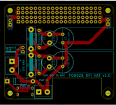
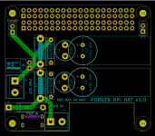
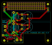
A prototype PO89ZB on a HAT for a Raspberry Pi
Thanks, Mark, and everyone else here who chooses to spend their time and energy having a look. So here it is, with some design notes.
I tried for 2.0mm tracks throughout, except where "steric hindrances" necessitated 0.6mm tracks or where routing on opposite sides of the board couldn't help. I'm not pleased about those 0.6mm traces, but the power-only surface mount USB-C receptacle, and the two stacked 40-pin GPIO ports in the standard locations for a Raspberry Pi HAT, don't allow for thicker traces to all pads. Power out through the upper block is relevant for directly powering an RPi through the GPIO when this board is the first board on top of a RPi. For use with HiFiBerry DACs, which is my preferred application, this board would be on top of the DAC and would connect and power both the Pi and the DAC through the lower GPIO block, which thankfully gets 2.0mm traces from the PO89ZB.
There are two power-in options (USB-c and a little screw block) and three power-out options (a horizontal jumper, a little screw block, and the GPIO blocks). I wanted jumpers to both +5V and GND to the GPIO so it could be isolated from the power out of the PO89ZB in case of experimentation or troubleshooting.
The board cutout is intended to accommodate the paired RCA jacks in HiFiBerry soundcards, which are a little too tall to allow this board to mount and connect through the GPIO bus if the board lacked the cutout. The capacitor rectangles are sized to accommodate the TDK capacitors I bought by accident which at 12.5mm x 25mm are a touch longer and wider than the 10mm x 20mm KEMETs and similars.
I don't have a ground plane (yet), or a board margin, or probably any of the other secret stuff a proper PCB layout needs. I was hoping that these images are enough to see if this looks square to you all, before I proceed with it and look into getting some prototypes made. Thanks again for your attention!🙂
Attachments
I should add, the official HAT spec includes voltage protection circuitry for anything that draws power from the GPIO. Since the whole point of this is to put power to the GPIO, I wasn't sure it was necessary. I've thought about adding a spot for a 5.1V Zener diode in parallel with the output lines to the GPIO but decided I didn't know enough to judge whether that would actually work to cap the voltage to or from the GPIO at 5.1V.
100:1 improvement
A friend of mine was looking into the possibility of using some inexpensive ($1.60) buck voltage converters for a project but they were so noisy he deemed them worthless. I suggested he try Mark's filter before he threw them away.
He was a bit puzzled (and perhaps skeptical) when he saw the resistors in parallel with the inductors, but tried it anyway. He couldn't get the resolution he wanted with the scope probes, so he soldered on a coax connector to connect the scope (he's a microwave engineer) and arrived at the attached photo, claiming that Mark's filter provides a better than 100 to 1 improvement in the signal.
Purple line is the input, but re-scaled so much you don't see all the noise.
Yellow line is the filter output.
He's impressed!
Way to go Mark!
Attachments


@ranshadow, "PO89ZB" is the identifier of my specific PCBoard layout. That's why the silkscreen text says PCB-ID: PO89ZB . See also post #406 in this thread. The idea is: there's only one PCB layout in the whole wide world with that ID, so there's no confusion.
I don't mind if you create a new board layout but please invent your own PCB-ID and don't reuse mine.
I don't mind if you create a new board layout but please invent your own PCB-ID and don't reuse mine.
@GnuB, microwave engineers spend their days working with "distributed parameter" circuits and devices, at microwave frequencies. Down here at "baseband" (audio), we have "lumped parameter" devices which may not be things he's thought about recently. The 953 ohm resistors in parallel with the inductors, handle problems that lumped inductors have, which distributed inductors do not.
Or you could just tell him, "hey the board is cheap. I don't mind if you cut out those two resistors with wire cutters and measure the response again. Have fun!"
Or you could just tell him, "hey the board is cheap. I don't mind if you cut out those two resistors with wire cutters and measure the response again. Have fun!"
@ranshadow, "PO89ZB" is the identifier of my specific PCBoard layout. That's why the silkscreen text says PCB-ID: PO89ZB . See also post #406 in this thread. The idea is: there's only one PCB layout in the whole wide world with that ID, so there's no confusion.
I don't mind if you create a new board layout but please invent your own PCB-ID and don't reuse mine.
Ok, happy to change it. I thought it was the suffixes that you mostly wanted changed.
@avdesignguru
Thanks for the perspective and the encouragement- it was you pointing me towards KiCad that got this going for me. Your earlier dimensions guidance on the current sense resistors was useful and I found a footprint in KiCad that I think matches, which I'm using for them. If you're curious, it's:
Resistor_THT:R_Bare_Metal_Element_L12.4mm_W4.8mm_P11.40mm
It was that last bit, the hole pitch, that matched.
I'm going to try JLCPCB for the simple reason that the USB-C receptacle I used in my design is one they stock and offer as an SMT option. It took some work to find a footprint for it and to make a symbol but I think all that is square.
@GnuB, ... you could just tell him, "hey the board is cheap. I don't mind if you cut out those two resistors with wire cutters and measure the response again. Have fun!"
Dang, great idea! Next board I give him will be missing them! 😀
It'll be fun to see the difference.
Thanks
Dang, great idea! Next board I give him will be missing them! 😀 It'll be fun to see the difference. Thanks
If you leave out the parallel inductor resistors, check out the response near 63MHz, since that is the self resonate frequency of those RLB0912-2R2ML inductors.
2*Pi*63MHz*2.2uH = Z = 870 ohms.
- Home
- Source & Line
- Analog Line Level
- PO89ZB, an inline DC filter for SMPS wall warts. Preamps, HPA, Korg NuTube, etc