Hi!
I purchased JVC A-X2 amp in mint condition.
After a few hours of listening the fuse has burnt. The amp was dusted inside and had original parts, I am sure it was not repaired/modified before.
I checked inside, and right OP transistors were burnt. I mounted A1943/C5200 instead but in both channels this time. After powering up I checked the voltage at OP trans bases, it was OK, I set the bias and let it warmed. After 15 minutes I connected the speakers and heard good quality sound of music. Until the first louder drum kick… then the amp smoked right channel OP and drivers trans this time. The left channel remained OK.
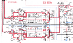
The picture from ltspice shows real measured voltages and some calculated currents.
The problems is, that I have +34.6V DC at the bases of the drivers.
I checked all of the parts on the pcb with the probe and it seems that the transistors were OK.
It looks like the current through Q4 is too small.
When measuring the voltages at the basis of Q1, Q2 and Q6 after connecting DVM it slowly lowered what was a bit strange because of high input impedance of DVM...
After some time those fluctuations were visible at right channel amp’s power indicator (-40 dB blinking) what was another mystery without OP transistors mounted…
Do you know what part is suspicious looking at the schematic?
Thank you in advance for any suggestions.
I purchased JVC A-X2 amp in mint condition.
After a few hours of listening the fuse has burnt. The amp was dusted inside and had original parts, I am sure it was not repaired/modified before.
I checked inside, and right OP transistors were burnt. I mounted A1943/C5200 instead but in both channels this time. After powering up I checked the voltage at OP trans bases, it was OK, I set the bias and let it warmed. After 15 minutes I connected the speakers and heard good quality sound of music. Until the first louder drum kick… then the amp smoked right channel OP and drivers trans this time. The left channel remained OK.
The picture from ltspice shows real measured voltages and some calculated currents.
The problems is, that I have +34.6V DC at the bases of the drivers.
I checked all of the parts on the pcb with the probe and it seems that the transistors were OK.
It looks like the current through Q4 is too small.
When measuring the voltages at the basis of Q1, Q2 and Q6 after connecting DVM it slowly lowered what was a bit strange because of high input impedance of DVM...
After some time those fluctuations were visible at right channel amp’s power indicator (-40 dB blinking) what was another mystery without OP transistors mounted…
Do you know what part is suspicious looking at the schematic?
Thank you in advance for any suggestions.
Attachments

That sounds like you are running into a too lower impedance. The speakers can be no lower than 8R per side.
The amp is intended to drive 4 Ohm speakers as well.
Left channel is perfect robust, I suppose the right should be too,
but now I cannot localize the source of +34.6VDC at drivers' bases issue... and this is my concern...
Left channel is perfect robust, I suppose the right should be too,
but now I cannot localize the source of +34.6VDC at drivers' bases issue... and this is my concern...
Check the fuseable resistors, they are designed to fail under stress. This amplifier is designed to drive 8R speakers NOT 4R!
See page 1 of the service manual under 'specifications'.
See page 1 of the service manual under 'specifications'.
that ltspice sch is not completed. but then again what is inside the super A bias part?
yes, it shows the actual situation, C5200/A1943 are not connected.
good, left channel measures +-1.7 V DC to the drivers while the broken channel +34.6 V DC to both of the drivers
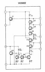
Your schematic for VC5022 is not correct one, it looks like a mix of VC5022 and VC5022-2. Hence, below is a complete VC5022 schematic for your reference.🙂
thank you very much for it!
however the manual JVC M-10 gives this (attached), even when I switch it off I cannot find broken part:
Attachments
Check the fuseable resistors, they are designed to fail under stress. This amplifier is designed to drive 8R speakers NOT 4R!
See page 1 of the service manual under 'specifications'.
Dear!
Thank you for helping,
OK, I burned the amp with (maybe) wrong load, please help to investigate which parts might be broken.
Partial incomplete LTSpice circuit was only to show actual measured voltages.
thank you very much for it!
however the manual JVC M-10 gives this (attached), even when I switch it off I cannot find broken part:
Attach is schematic for VC5022-2🙂
that ltspice sch is not completed. but then again what is inside the super A bias part?
attached is workable amp but as Aparatusonitus pointed out, Super A section with VC5022 has errors,
but again, which part is suspicious to give +34.6 V DC at OP trans drivers?
Attachments
I'd check those two 180R flameproof resistors (R12/13 in your sim). If those measure OK, I'd say Q4 is toast.
I'd check those two 180R flameproof resistors (R12/13 in your sim). If those measure OK, I'd say Q4 is toast.
R12/13 are OK,
Q4 desoldered measured well
but I agree it is main suspicion, when powered with higher voltages than hfe DM it might leakage/open, I will change it!
Thank you very much!
Attach is schematic for VC5022-2🙂
there is not possible to set the bias <6A even with shorted bias multiplier with the "right" version of VC5022, asc attached
Attachments
Delete Q18 and R34 connect Q17 collector to Q7 collector...
no 😉
VC5022 sch sent by you http://www.diyaudio.com/forums/solid-state/300164-please-help-repair-jvc-x2.html#post4905558 contains the error, Q4 on that schematic should be NPN type, not PNP, and this I changed in attached asc,
now the sim is OK,
and in this way the amp should behave,
but it is not😱
Q4 on my sim/X605 in original sch is OK, checked😕
Attachments
Spot on, Eagle Aye😉...But as I have suggested in the previous versions with a single transistor constant current sink/source for the upper and lower branch of variable bias circuit will work as intended. In your version (which is probably more accurate than mine), you effectively replaced one transistor for CFP-Compound Feedback Pair (aka Sziklai pair). May I suggest to put another resistor (value from 1k2-3k9) from Q17 collector/Q18 base junction to Q7 collector in order to avoid possible oscillation in CFP...do the same for upper and lower branch.🙂
Spot on, Eagle Aye😉...But as I have suggested in the previous versions with a single transistor constant current sink/source for the upper and lower branch of variable bias circuit will work as intended. In your version (which is probably more accurate than mine), you effectively replaced one transistor for CFP-Compound Feedback Pair (aka Sziklai pair). May I suggest to put another resistor (value from 1k2-3k9) from Q17 collector/Q18 base junction to Q7 collector in order to avoid possible oscillation in CFP...do the same for upper and lower branch.🙂
Hi!
I think that JVC made (non)intended mistake with this Q4 type on the information sent by you.
found!
Hi guys!
VC5022 is shorted/open between some pins compared to the one in good channel, and this was the reason for getting strange voltages at the drivers.
I ordered already new one and will let you know about further repair progress!
Hi guys!
VC5022 is shorted/open between some pins compared to the one in good channel, and this was the reason for getting strange voltages at the drivers.
I ordered already new one and will let you know about further repair progress!
I ordered already new one and will let you know about further repair progress!
Blasphemy...you should build your own (better, of course) with discrete part

- Status
- Not open for further replies.
- Home
- Amplifiers
- Solid State
- Please help repair JVC A-X2