I would like to ask why very large public address amplifiers often employ two complementary input stages? Using two different sub-circuits for the input necessitates that the two sub-circuits behave exactly in the same way. My impression, which may be wrong and that is why I am asking, is that, making NPN and PNP transistors to match to a very high degree, is expensive and difficult.
Last edited:
The type of input stages I am asking about employs a current source, a differential pair and optionally a current mirror. I am not asking about balanced inputs, which would need an op-amp before the actual power amplifier input.
Double input stages like this are typically used to drive a push-pull VAS. Why a push-pull VAS is another question of course!
Its complementary, not complimentary.
Its complementary, not complimentary.
From different circuits employing such input stages, it is clear the two input stages work in opposition. While the output (transconductance) current increases in one input stage, in the other, it decreases. Therefore, one transistor in the VAS becomes more conducting while the other becomes less conducting. My logic tells me this should increase the voltage gain of VAS compared to having only a current source instead of two transistors working in opposition. The advantage seems to be having a VAS that is actively driven to both rails, instead of relying on a current source to pull the VAS towards its reference rail.Double input stages like this are typically used to drive a push-pull VAS. Why a push-pull VAS is another question of course!
You haven't provided an example circuit leading to various interpretations of the question. Current source stages do not have symmetrical slew rates (in general). This affects distortion at HF.
Matching of transistors is not an issue if DC trim or servo is implemented and is also assisted by current mirrors.
Matching of transistors is not an issue if DC trim or servo is implemented and is also assisted by current mirrors.
Current source stages do not have symmetrical slew rates (in general). This affects distortion at HF.
Unlikely in a competently designed amplifier.
Competent is an arbitrary judgement. Asymmetry can be seen in many designs and is more manifest into reactive loads. The difference in waveform triangulation can be seen between rising and falling edges as the frequency rises. Even if the measured rise times may be similar, the shape of rising and falling edges differ. A significant number of designs never make to their -3dB bandwidth limit without signal triangulation into reactive loads. Are these designs competent?
Some favor symmetrical topology for this reason.
Some favor symmetrical topology for this reason.
A significant number of designs never make to their -3dB bandwidth limit without signal triangulation into reactive loads.
Slew rate, and triangulation thereof, is not a function of the load at the amplifier's output. The slew rate of an amplifier is a function of the input stage's quiescent current, the second stage's quiescent current, the size of the amplifier's compensation capacitor and the value of the amplifier's internal parasitic capacitance, especially at the output of the second stage.
I think it is just a matter of "perfect symmetry" of the schematics. And the second path adds impressive 6db loop gain!
Thus not worth the complexity imho.😉
Thus not worth the complexity imho.😉
Last edited:
Slew rate, and triangulation thereof, is not a function of the load at the amplifier's output.
Yes it is. As the current draw of the output devices increases, the beta of BJT falls requiring more current from the drivers. Therefore the load has a ripple effect into the earlier stages of the design. Capacitive loads demand a lot of current. A simple simulation in LTspice proves the point. Distortion variance with load also proves the point. If your amplifiers are completely immune from load, that is a good trick.
There is a schematic with two input stages in post 48 of the thread: Single or dual differential?
There is another post 8048 in the thread: Bob Cordell's Power amplifier book
There is another post 8048 in the thread: Bob Cordell's Power amplifier book
Last edited:
They could be competent if they are never driven into that misbehavior and don't display it when operated within their capabilities. If the amplifier is overdriven, then all bets are off regardless of design.
Yes it is. As the current draw of the output devices increases, the beta of BJT falls requiring more current from the drivers. Therefore the load has a ripple effect into the earlier stages of the design. Capacitive loads demand a lot of current. A simple simulation in LTspice proves the point. Distortion variance with load also proves the point. If your amplifiers are completely immune from load, that is a good trick.
Capacitive loads do not necessarily "demand lots of current": the current drawn by a capacitor depends on the signal frequency and the value of the capacitor. In any case, the load at the output of a competently designed amplifier should not have any effect on its slew rate.
Someone once said "The less people know the more stubbornly they know it", an apt aphorism methinks as you seem impervious to the truth. Perhaps some civic-minded person will step in here to enlighten you. Alternatively, you would educate yourself no end by reading a good textbook on elementary linear electronics theory.
I think the first commercial version of what you cite was Jim Bongiorno's Ampzilla.
Here's a link to the 1974 article:
https://www.updatemydynaco.com/HistoricDocuments/ampzilla_web.pdf
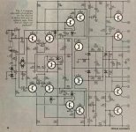
The picture here is the Ampzilla front end from that article.
Here's a link to the 1974 article:
https://www.updatemydynaco.com/HistoricDocuments/ampzilla_web.pdf
The picture here is the Ampzilla front end from that article.
Attachments
Subject an amplifier to a standard square wave test signal and 8R+2uF load and tell us what the peak current reads.
edbarx, the reply I initially offered remains valid. The vbe of the input transistors is controlled by the value of the emitter resistor. The matching problem moves to how well the emitter resistors are matched and how accurate the current mirrors perform.
Input offset voltage is cancelled by the opposing base currents of the NPN and PNP devices. If one device's base current is double the other, the input offset voltage is still only the same value, or less, as if one device was used. What also helps is a low input impedance so that differences in base currents have less contribution to the offset voltage, same as for one device.
The current mirrors may need some effort for matching. This is sometimes done by altering the emitter resistors of the NPN and PNP current mirror transistors instead of device matching. Modern complementary devices can have good matching.
Does any of this address your initial question?
Perhaps some civic-minded person will step in here to enlighten you.
Certainly not you, Worldie, you seem hell bent on trying to punish people who ask a little more information.
I'm always amazed how many incompentent amplifiers there are in the world. Incredible that so many seem to work!
- Home
- Amplifiers
- Solid State
- Please, explain why two complimentary input stages.