Alan, pleased to hear that you have drawn a line in the sand and are (nearly) at the stage of actually building something. Can you give us some details of your fully balanced input stage. I hope you are going to produce something that is true to the design of your favourite YBA amplifier, but with your own twist.
Sent from my iPad using Tapatalk
Sent from my iPad using Tapatalk
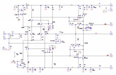
The IPS VAS is just the same I posted in all the simulations in other threads with balanced complementary IPS. It is very close to the YBA except I still have the cascode for the LTP. I can always jumper the cascode to make it true YBA that give slightly higher 2H and slow it down a little!!!Alan, pleased to hear that you have drawn a line in the sand and are (nearly) at the stage of actually building something. Can you give us some details of your fully balanced input stage. I hope you are going to produce something that is true to the design of your favourite YBA amplifier, but with your own twist.
Yes, there are times to keep talking and thinking, but there comes a time that I have to make a decision and go with it.
Actually you have strong influence on my OPS. I originally use all NPN and PNP on the top and bottom resp. A lot of other people do that. But something did not feel right for me. Bias multiplier has to do 6Vbe, idle current is very sensitive to change of resistance in the divider. More importantly it is impossible to put the transistor of the bias multiplier at a place that truly can sense and compensate the temperature drift. That's the reason I kept posting the schematic and not sending it out even I finished the layout. After looking at your design, that tipped me over to the PNP NPN NPN and NPN PNP PNP 3EF. Then EVERYTHING came together. I can couple the pre drivers with the drivers on a separate heat sink to get close thermal tracking and as short a lag time as possible. Then I can put the transistor of the bias multiplier on top of one of the big output transistor to get close coupling also.
Also AndrewT's comment on putting the power transistors in NPN PNP NPN PNP on the layout pushed my over to put it that way instead of all PNP on one side and NPN or the other sid. Everything comes together, I did not have to compromise anything in the layout. I think this is as good as it get and I feel very good about it. I am sure engineering wise, it is sound, the question is just whether it sounds good or not!!!
I might have to delay building the amp a little. All of a sudden, my former company that I work for almost 10 years ago before I retired call me and ask me to do a two months contract with them in designing some RF circuits for their mass spectrometer!!! That will give enough pocket money to build many amps!!! I have to go in and talk to them and see what comes out of it.
Thanks
Last edited:
False alarm about the lost package. I read the wrong package delivery, that was for a bench power supply. I received it today. BUT my comment on Allied Electronics stands. They are so slow, it's been 3 Weeks before I received the package.
Sent out the IPS/VAS already, now deciding whether I want to make a pcb for the filter caps as it's so cheap!!!!
Sent out the IPS/VAS already, now deciding whether I want to make a pcb for the filter caps as it's so cheap!!!!
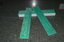
Received the OPS pcb today. The others will be coming soon. But I just got a contracting job offer, so it's going to be a little while before I get to it.
Still have not received the last package from Allied electronics. Don't order from them.
Still have not received the last package from Allied electronics. Don't order from them.
Attachments

Last edited:
ThanksGood looking boards Alan, congratulations!
The other boards are going to arrive in a few days. Right now, I am designing the pcb for the preamp chassis. The one that select inputs from different DVD recorders and VCRs and mux to the tv and power amp. I am using Ti LM4562 opamp as buffer and just using a 4P3T rotating switch to switch the audio and video signals. If you have better suggestion, let me know.
I want to sent this board out before I go to work.
Ha ha, that's how I work, I spend a lot of time thinking, talking on the forum, weighting the pros and cons before I even start the design. But once I get going, it's very fast. I already sent out 4 boards and this is the last one for the preamp.
Other than the last shipment from Allied, I have all the parts in house. I made a mistake double ordered the MJL3281, now I have 70!!! I have 45 of the MJL1302. I hope I can pick out a few sets of closely matched sets of 5 transistors!!! That's $350 right there. Should last me a few amps.
Building your own amp does not necessary cheaper, just hopefully is better!!! I bought and received two 24V 15A switchers, I burned them in already, I am going to use it as power supply for my first prototype, then I can up the current to say 300mA per stage. This will give 1.5A bias current and 3A peak class A current. For 4 ohm speaker, it will be 12V or class A. This will give me 0.5 X 12 X 3= 18W of Class A power!!!
Last edited:
I doubt any commercial amp will come close to matching the performance of what you are building here for under $1k.
I know what you mean about accidentally over ordering parts. I accidentally ordered 50 power MOSFETs when I meant to order 5 !
Can you post the schematic and layout for your input stage? I am finalising another fully balanced pcb and wanted to compare notes...
I know what you mean about accidentally over ordering parts. I accidentally ordered 50 power MOSFETs when I meant to order 5 !
Can you post the schematic and layout for your input stage? I am finalising another fully balanced pcb and wanted to compare notes...
Here is the schematic and layout of the IPS VAS
Attachments
- Status
- Not open for further replies.
- Home
- Amplifiers
- Solid State
- Please comment on my OPS design