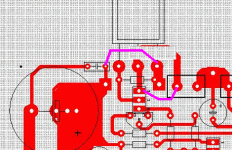
please comment my pcb
zobel network is to be located at outpout connector and return to star ground with a separate cable
An externally hosted image should be here but it was not working when we last tested it.
zobel network is to be located at outpout connector and return to star ground with a separate cable
Hi Sakis,
The only problem I suspect is if you are making two of these to run off one PSU. If you are you need two ground returns to the PSU star from each PCB. Otherwise the two channels will interact.
If not it's OK
The only problem I suspect is if you are making two of these to run off one PSU. If you are you need two ground returns to the PSU star from each PCB. Otherwise the two channels will interact.
If not it's OK
Hi,
Looks good! Very nicely organized.
One thing:
You have the input ground direct to the power ground?
Looks good! Very nicely organized.
One thing:
You have the input ground direct to the power ground?
strangelly yes
in fact most of times i did this i had less problems than running ground through 10R resistor
MJL21193 said:Hi,
Looks good! Very nicely organized.
One thing:
You have the input ground direct to the power ground?
in fact most of times i did this i had less problems than running ground through 10R resistor
Hi Sakis,
I have tried various stereo layouts similar to your last post and I could never get them hum and buzz free.
A monobloc where the Audio Ground is on the PCB works OK, but not when you connect more than one channel.
I don't see your schematic but I wonder if the NFB route sends the inverting input from the correct end of the second (lower leg) resistor?
On the same NFB route, it appears to be tapped off the emitter resistor instead of from the speaker output.
Re: this the config

This is like polluting your drinking water by connecting the toilet to the water well.
Set up an input signal ground that is isolated from the main power ground.
Return the speaker ground to the main power ground, not on the amp board but on the power supply board. Return the Zobel here too.
sakis said:i have in mind
never tryied that exact config but will see when pcb is ready
This is like polluting your drinking water by connecting the toilet to the water well.
Set up an input signal ground that is isolated from the main power ground.
Return the speaker ground to the main power ground, not on the amp board but on the power supply board. Return the Zobel here too.
well andrew
i had the exact same configuration ....but all done on a pcb and the amp was the most quiet ive listen to my all life ....
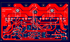
lets see if i can get you a photo of that
it was made with the exact same config and the only diference was that C and R part of zobel was located on board and return to the local star ground of each amp
otherwise it was the complete same
i had the exact same configuration ....but all done on a pcb and the amp was the most quiet ive listen to my all life ....
lets see if i can get you a photo of that
it was made with the exact same config and the only diference was that C and R part of zobel was located on board and return to the local star ground of each amp
otherwise it was the complete same
Attachments
Re: Re: this the config
ok ok give me a brake man ..... said never tested this before will do and also listen to all advice
look at the pcb above its ultra quiet but zobel is located on board ...and local star ground
MJL21193 said:
This is like polluting your drinking water by connecting the toilet to the water well.
Set up an input signal ground that is isolated from the main power ground.
Return the speaker ground to the main power ground, not on the amp board but on the power supply board. Return the Zobel here too.
ok ok give me a brake man ..... said never tested this before will do and also listen to all advice
look at the pcb above its ultra quiet but zobel is located on board ...and local star ground
Hi Sakis,
Don't take offense, I don't mean any. Lots of reading here (the man above, AndrewT) and experimenting with different amp builds shows that the best way is to separate the grounds. You don't want noise from the common ground polluting the signal ground.
Don't take offense, I don't mean any. Lots of reading here (the man above, AndrewT) and experimenting with different amp builds shows that the best way is to separate the grounds. You don't want noise from the common ground polluting the signal ground.
no ofence dont worrie
mostly jocking ....
the thing is that this amplifier i listen too every day in my shop ultra quiet and performs square wave up to 30khz with no probs
no signs of hum buz or any oscilation or interference at this range of frequency ....
but will see though pcb is going to ready in few days
one way or the other after this set up ground rooting can be done in many many alternative ways so will find which one is the best
Re: no ofence dont worrie
and the easiest way to give this flexibility is to have a separated Signal Ground from the power Ground on the PCB. Keep them next to each other and allow for a shorting link/resistor to connect them for your first experiment. If it works as a two channel then great, come back and show us how to do it.sakis said:one way or the other after this set up ground rooting can be done in many many alternative ways so will find which one is the best
give it some time
thepcb factory normally takes a week to produce this
will make it and get back to you
thanks though
thepcb factory normally takes a week to produce this
will make it and get back to you
thanks though
This layout contains most of the usual mistakes. They are repeated again and again by everybody because linear amplifiers are so forgiving.
The small films wired in parallel with the big electrolytics through long and thin tracks are particularly useless and potentially harmful, you really know how to make RF resonators with PCB inductance. You will be lucky if the resonant frequency of these RL does not fall close to amplifier unity gain crossing because this leads to instability.
The extra-long ground tracks around the board are another usual and funny mistake. You usually complain of the inductance of big electrolytics, which is roughly 15nH for parts with 10mm terminal spacing, negligible for linear amplifiers, but you always forget PCB inductance which easily becomes 10 or 20 times higher (unless tracks are kept ultra thick and really short and/or a ground plane is employed).
Optimum amplifier layout is the opposite. Place the power stuff in one side of the board with short tracks, power and signal connections near the middle and the small signal stuff on the other side. Never place the small signal stuff in the center and the power stuff around it at the sides, this results in maximum interferecne and the worst PCB parasitics.
thanks for join in Eva
i wonder if this all is audible
can we compaire for a minute this pcb with average yamaha or pioneer amplifier pcb ????
whats the catch here ???
am i missing something ????
cause if we follow this logic all these pcb we ve seen is to be thrown in the garbage.... Plus that this is no sophisticated amplifier i have no expectation to listen 150khz sounds from it ...
thanks though, i will consider a revision under these specs
- Status
- Not open for further replies.
- Home
- Amplifiers
- Solid State
- please comment my pcb