Eva said:This is a good layout, it more or less follows my guidelines. No wonder THD is low 😉
0.0001% THD-20 from this class AB output stage:
http://www.synaesthesia.ca/OP-stage.html
Would be hard to put the +/- supply tracks further apart. Non interleaving of the P/N channel devices also.
G.Kleinschmidt said:
Practical mechanical layouts in high power audio amplifiers will always limit one to less than theoretically ideal PCB layouts.
But that not always matters too much or is the end of the world.
Hi Glen,
It's not going to keep me up at night, for sure. Nothing can be perfect and unfortunately everyone picks on the short-comings and ignores the good points. The short-comings in my case are very tiny and have little (or perhaps none) impact on the overall performance. A good test for any amp is how stable it is into different loads and I demonstrated that mine held up nicely. It's in my thread for anyone to see.
I will heed good advice and make use of the improvements offered. It would have been better if I had this knowledge before I finalized that layout. It all goes into the books for later use. 🙂
In the meantime, I will strive to get my layout and design THD tested to see just how badly I botched it up by putting the power leads at opposite ends. My uneducated guess would be "not much".
G.Kleinschmidt said:
It's the whole amp that has 0.0001%. The output stage has about 0.008% and the PCB has a ground plane on the top layer. But then I agree that this PS lines layout is overestimated. The YAP http://www.diyaudio.com/forums/showthread.php?postid=1595560#post1595560 power stage has a THD20 of 0.002% and uses the same type of layout as the PGP.
Although I probably should, I can't decide to put the filter caps on the power stage board, to resolve the high the currents locally. It's to expensive (from a PCB perspective) and I'm to lazy to start doing in house PCBs.
mjl21193 . Glen .....
may some of you didnt lost your sleep over this but actually i did regarding my own pcb and related issues ....
after carefull thinking i agree 100% with Eva to all the points mentioned .....
All except one : Eva thinks that the power traces simply work as resistors that "swing" cause of ower suged by the amplifier and this is not nice to have next to your LTP for example ....
I think that this apply to pcb that dont have elctro's on board ....but thats me this is the way i think about this ....
then again as about all the rest that find me 100% agreed after very carefull trying with my pcb layout software i realized that if you need to cover all Eva's specs ( and mine also ) you need a double layer pcb ....
Question rizes """" does a P3A amplifier worth a double layer pcb ????"""""
cause if you invest money in double layer PCB you migth as well make a better amplifier ....
syn08 said:
It's the whole amp that has 0.0001%. The output stage has about 0.008% and the PCB has a ground plane on the top layer. But then I agree that this PS lines layout is overestimated. The YAP http://www.diyaudio.com/forums/showthread.php?postid=1595560#post1595560 power stage has a THD20 of 0.002% and uses the same type of layout as the PGP.
Although I probably should, I can't decide to put the filter caps on the power stage board, to resolve the high the currents locally. It's to expensive (from a PCB perspective) and I'm to lazy to start doing in house PCBs.
Yeah, I know it's the whole amp that does 0.0001%. I should have written 0.0001% from the amp using this OPS 🙂
Agreed about the power supply lines / OPS routing. The most important factors when laying out a power amp PCB are grounding and splitting / keeping the small signal stuff away from the high current stuff.
My personal preference is for using local bypassing on the PCB and keeping the main supply filter capacitors off. That keeps the bridge rectifier currents away.
Cheers,
Glen
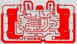
Eva said:Are you blind or what?
Supply rails are connected and laid out together through the center of the board, and decoupling capacitors are also placed together on the center.
Edit:
Note the quasi-ground-plane arrangement: The supply rail traces are on the top side while the speaker output and return traces are under them on the bottom side following the same path to reduce inductance and coupling to small signal circuits.
A few more points:
It doesn't matter a jot that the capacitors are close together in the middle of the board instead of on either side as the capacitors connect after the rail fuses which are located at either side of the PCB, so the track lengths/loop are no better off.
Ultra-LD MKI

With the exception of having the supply rail traces run on the top of the PCB this time, the output stage layout is identical to several of their previous designs, including the “Studio 350”, which can be seen clearly here:

And no, the speaker return current does not follow the same path as the supply rails. In fact it nicely wraps up half of the small signal circuitry (LTP and VAS current sources) and the heavy half-wave earth return currents of the filter capacitors flow smack-bang right through the small-signal circuity via the earth return track down the middle of the board.
The PCB layout of my 12W amp that I posted earlier, with the central star ground well away from the small signal circuitry is "theoretically" superior to this.
Cheers,
Glen
Oh, and another thing.....
Two lengths of supply rail tracks overlaid on a PCB (top/bottom layer) that conduct alternate half cycles (180 degrees) radiate the same magnetic field as a single track conducting the full cycle (360 degrees) - When the current in one track is zero, there is no opposing field to cancel that of the other.
Cheers,
Glen
sakis said:may some of you didnt lost your sleep over this but actually i did regarding my own pcb and related issues ....
after carefull thinking i agree 100% with Eva to all the points mentioned .....
Question rizes """" does a P3A amplifier worth a double layer pcb ????"""""
cause if you invest money in double layer PCB you migth as well make a better amplifier ....
Hi Sakis,
The biggest flaw with your layout was the grounding and that was pointed out before Eva came along.
Any layout can be made single sided. My own is more complex than the P3A and I easily managed a SS layout.
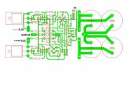
I have done some changes to try out some of the suggested improvements and the result is below. Power in and rail decoupling have been moved to the centre, in close proximity to the ground and speaker out connectors. A few more hours (
 ) of layout fun will tidy everything up.
>>>>I can't attach the pic. I'll show it later.
MJL21193 said:
>>>>I can't attach the pic. I'll show it later.
I'll do it this way:

Am I on the right track?
a couple of things
i would never do ( was actually pointed to you before )
A) ground is a trace that is almost a circle arround the pcb .I dont like it and i thing Eva doesn't also )
B) Some traces are too close too eachother .The gap between them is too litle
C) Too many parallel lines also too close to eachother
D) finally i thing that mooving decoupling next to transistors will effect almost nothing compaired to the things i ve spoted .
on the other hand dear MJL as mentioned above there is one part i dont agree with Eva and some others that i totally agree 100%
so there is a question of opinion and the way we like to do things no hard feelings i presume
but this is not the way i like it
( notice that previous pcb ive made had various mistakes but none of the above )
freindly constructive regards !!!!!😀 😀 😀
Re: a couple of things
That pic is early again as I'm not finished yet, but that ground trace is only for the input signal ground and doesn't carry large current. It doesn't have any impact on the rest of the circuit. It's not the same as putting the input right on top of the star ground like you did.
??? The gap between traces is fine.
Have you looked at any other layouts? They all have parallel traces, it's impossible to avoid unless you make a huge wasteful board (like yours 😀 ).
Those were the suggested changes. I could be stubborn and refuse to change anything, ignore good advice and stumble forward with my eyes closed like some others, but I prefer to say I'm not as well knowledgeable as some pretend to be.
Anyway, judging by your responses you obviously don't like to "share" your thread and I'll accept that. I'll take down the pic I attached and leave you to it.

sakis said:i would never do ( was actually pointed to you before )
A) ground is a trace that is almost a circle arround the pcb .I dont like it and i thing Eva doesn't also )
That pic is early again as I'm not finished yet, but that ground trace is only for the input signal ground and doesn't carry large current. It doesn't have any impact on the rest of the circuit. It's not the same as putting the input right on top of the star ground like you did.
sakis said:
B) Some traces are too close too eachother .The gap between them is too litle
??? The gap between traces is fine.
sakis said:
C) Too many parallel lines also too close to eachother
Have you looked at any other layouts? They all have parallel traces, it's impossible to avoid unless you make a huge wasteful board (like yours 😀 ).
sakis said:
D) finally i thing that mooving decoupling next to transistors will effect almost nothing compaired to the things i ve spoted .
Those were the suggested changes. I could be stubborn and refuse to change anything, ignore good advice and stumble forward with my eyes closed like some others, but I prefer to say I'm not as well knowledgeable as some pretend to be.
Anyway, judging by your responses you obviously don't like to "share" your thread and I'll accept that. I'll take down the pic I attached and leave you to it.
john .....
come on now .....THIS IS JUST A MATTER OF OPINION !!!!!
this is the way I like to do things .....it doesnt mean that it s correct also ....
never the less dont forget that circuits iam working with is much more simle so may be this all apply to my circuits and yours that is more complicated canot be done otherwise ....
i have no problem with you jumping in the thread presenting your pcb ....( i actually welcome others since looking at various aproach might give us a better idea )
and most of all dont be pissed off cause all this ....its just a matter of opinion .... may be after all you are right....
i don;t know ....if knew i will post like GLEN ....
"""" this is the circuit ...and pcb ...its just for you to see not to judge i am not willing to change anything """""
just a joke GLEN .... i try to see things with happy funny view
as about the pcb ....well i insist that it can be done in some other way
A)Look at Q10 do still belive that the trace of speaker rail and ground is ok to have this gap betwen them ???? i still belive that needs to be more .....i thing like in this area the speaker rail and ground rail is just a big capacitor (may others see and tell us i amnot really sure what i am talking about .....it doesnt look nice to me )
B) the reason i dont like the ground trace all around the pcb almost a circli is that i feel that this will work as RF antena and pick up RF insome very weird high frequency ( please others may express their opinion about this)
C) and finally look arround R22 or R2 or C7 in these areas i thing that these too many paralel lines dont look nice from parallel view and also from proximity view i still beleive that these will work as capacitors .....C12 also .... i dont like the trace down under the cap .....
but yet again ..... this is a matter of opinion ....there is no reason to get upset about it ....
this is a happy friendly thread which from all may learn !!!!!!!!!!!!!!
Re: john .....
Hi sakis,
You jump on my low current ground trace (no one has criticized it, not even Eva) but you, yourself have done exactly what you said you would never do - create a ground trace that circles the board! Remember your board layout from post #1?? See pic below.
As for parallel traces and spacing look at the example that Glen presented above. That's a commercial amp. Look at the pics Eva posted. Look at the spacing of the traces and the parallel traces.
I can deal with constructive criticism. I welcome it. I don't have time for nonsense nit-picking though, opinion or not.
sakis said:i would never do ( was actually pointed to you before )
A) ground is a trace that is almost a circle arround the pcb .I dont like it and i thing Eva doesn't also )
sakis said:
B) the reason i dont like the ground trace all around the pcb almost a circli is that i feel that this will work as RF antena and pick up RF insome very weird high frequency ( please others may express their opinion about this)
Hi sakis,
You jump on my low current ground trace (no one has criticized it, not even Eva) but you, yourself have done exactly what you said you would never do - create a ground trace that circles the board! Remember your board layout from post #1?? See pic below.
As for parallel traces and spacing look at the example that Glen presented above. That's a commercial amp. Look at the pics Eva posted. Look at the spacing of the traces and the parallel traces.
I can deal with constructive criticism. I welcome it. I don't have time for nonsense nit-picking though, opinion or not.
Attachments
john....
i can still see that you are upset about it ....i really dont see the point ....
in this pcb that you have in your hands which its probably possible to be done since its much more siimple than yours first of all there is no resistor from star ground to signal ground ( this is the way i ve done it in the past and had no problems ) so actually this is part of the main ground ...this ground is not differential ....
on the other hand if you noticed arround the amp is the main caps and decoupling before and after them for example there is no parallel line ( except rails with not so much proximity like yours ) that comes in "conduct" with the ground ....it is very possible since so many caps are there , ground is not a complete circle , ground is very far away from anything else that your ground scheme and mine will behave totally diferent ..... better ?????? i cannot really tell
also since main caps are located on board for sure the all thing will behave diferent than yours ..... if better i really dont know ....
finally as long as Eva spoted that and a few other things i said that i am going to change it ....still dont have the time since i am very busy .....
as i said before if you need to fullfill Eva's specs about basic pcb construction (power ,out, ground, decoupling next to transistors one side ----other side input and small stuff ) and then the rest of genneral audio rulls ......and then mi "thingy " about very symmetric looking pcb ......its not an easy thing to do in a single layer ......
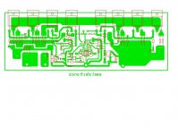
this is
more or less what i had in mind
please notice this generic not complete yet
------ compact and symmetric
------- decoupling next to transitors
-------rail traces small and located in the output side
-------as less parallel lines as possible
-------small stuf away from power area
-------star ground
-------option to have pcb with caps on board also
Attachments
- Status
- Not open for further replies.
- Home
- Amplifiers
- Solid State
- please comment my pcb