That could be. Conditionally stable circuits have the reputation that they are more prone to get unstable at start-up or during clipping, but I have seen conditionally stable circuits that started up fine and recovered well from clipping, and unconditionally stable circuits that burst into oscillations and never stopped when driven into clipping. In general, small-signal stability is no guarantee for large-signal stability.
Hi Jan,
These seem reliable from a contact standpoint, but unless they are fully seated on the mating pins they are not that stable - may not be a big improvement over what you are using. When I am sure all is well I usually secure with a dab of hot melt glue.
www.digikey.com/en/products/detail/sullins-connector-solutions/PPPC051LGBN-RC/775938
This is the current version of the connector I have been using.
Looks better than what I have. Thanks.
Jan
Reading through all of the comments this reminds me of how much I have still to learn. Henry is a close friend and I tend to listen carefully to what he has to say.
When I have a little bit of time over the holidays I will build up a pair of my TPC op-amp modules and do some measurements with my RTX-6001, I think Jens will enjoy this from several perspectives - it is the only device I have that is likely to meaningfully exceed the performance of these op-amps.
In the mean time I have a version I have not shared here because it's simply the transconductance output design with my take of the diamond buffer appended, as I recall open loop gain is around 90dB or so.. Versions 3 and 4 (both here) have substantially more loop gain, but V3 relies on miller compensation and has a cascode tail CCS on the jfet front end, the V4 ditches the cascode tail and adds TPC.
Thank you for all of the feedback and commentary, I'm learning - lots of good thoughts and suggestions for me to study. Talking of such what are people's thoughts on the cascode tail CCS - benefit or waste of a transistor? What benefits beyond common mode behavior, and is this worthwhile given the inherent imbalances in this matched pair, when is it enough?
I am happy to report I will be mailing a pair of blank boards to an interested member in a few days, and still have one more pair to hand out if anyone is interested.
It would be cool if you could generate some schematics and Bode plots. It would make things clearer.
Hmm, let me see what i can do.
The Hire: Star (BMW short film starring Madonna) HQ - YouTube
That is correct. It is always nice to see the RTX6001 being put to good use.🙂When I have a little bit of time over the holidays I will build up a pair of my TPC op-amp modules and do some measurements with my RTX-6001, I think Jens will enjoy this from several perspectives - it is the only device I have that is likely to meaningfully exceed the performance of these op-amps.
In the mean time I have a version I have not shared here because it's simply the transconductance output design with my take of the diamond buffer appended, as I recall open loop gain is around 90dB or so.. Versions 3 and 4 (both here) have substantially more loop gain, but V3 relies on miller compensation and has a cascode tail CCS on the jfet front end, the V4 ditches the cascode tail and adds TPC.
Thank you for all of the feedback and commentary, I'm learning - lots of good thoughts and suggestions for me to study. Talking of such what are people's thoughts on the cascode tail CCS - benefit or waste of a transistor? What benefits beyond common mode behavior, and is this worthwhile given the inherent imbalances in this matched pair, when is it enough?
If the distortion of your op-amp is very low, you may have to use the trick of increasing the noise gain or use a very low distortion oscillator + notch filter to measure it correctly.
Have you considered using cascodes on the two FET's? E.g., a couple of low cost JFET's? It could reduce the input capacitance considerably.
It would be cool if you could generate some schematics and Bode plots. It would make things clearer.
Ok, let's talk in detail.
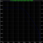
First image named "Simple" shows a schematic of a simple amplifier with a gain of 1. And second image, named "Without correction", shows its Bode plot. As you can understand it will be unstable.
First way to make it stable is Miller capacitance inserted around Q1+Q3 stage (usually named as Beta-enhanced VAS, but let's talk about later).
Let me doesn't show sch and go straight to Bode plot.
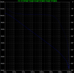
It's represented in the image named "100p" and it's ugly.
Doing this we just loose 60 dB of feedback depth at 20 kHz with tha same THD rise. This is exaxtly what is named "harsh transistor sounding".
Ok, let's try second order around VAS.
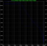
Corresponding Bode plot image is named 47p-1k-47p. This is a CRC nominals settled around VAS.
Wow, we can keep mostly all feedback depth at 20 kHz. Perfect!
Some optimisation are needed, but it's a unity gain and must be coorrected at needed external gain.
But what exactly we do? Not only feedback around VAS. Really this circuit must be seen as four stage amplifier and just try to understand this as two high-impedance points. First high-impedance point are placed between Q2 collector and J2 drain while second are placed between Q3 collector and I2 current source.
47p-1k-47p circuit not only provide feedback path around Q1+Q3 VAS. It also shunts the impedance of the both high-impedance points.
And while first of the high impedance point are stable (because it's signal them amplified around 1000x times in the second point) the last point have not only shunted. It's also loaded at changing capacitance of the last follower stage.
Let's try not to shunt VAS.
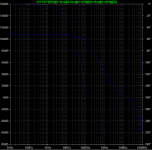
Schematic are shown in the image named "higher order_SCH" and corrsponding Bode plot in the image "higher order".
What do we see here. Firstly - much more HF gain, at least 20 dB feedback depth at 200 kHz which result mainly in a way less intermodulation distortion.
Second - a way better stability margins at a comparable unity-gain frequency.
Third - VAS load impedance dominated by known and intrinsically stable values (IPS output can also be stabilized, yes)
Fourth - OPS distortion are also accounted and corrected because all feedback are taken from the output.
That is i vote for.
Attachments


Thanks for the detailed explanation. Everything you say makes sense and is defensible. But there are always tradeoffs and I don't know how to evaluate them. For instance, removing feedback from around the VAS leaves more loop gain for global error correction, but at the cost of increased VAS distortion. The VAS collector is a high-impedance node, but maybe not as high as you think, depending on the Early voltage of the device. Reduced local feedback makes the VAS transfer function more dependent on the transistor's gain variability and nonlinear output capacitance. I can't say how that affects sound quality.
Referring to the paper you linked earlier, your approach is good for integrated op-amps where you can't get at the internal nodes for compensation. This isn't a constraint for discrete designs. I don't know what the pros and cons are of moving some of the loop compensation to the external feedback network, versus applying it to the forward gain path.
All of the papers I've read about two-pole compensation point out the increase in available loop gain for feedback, but don't mention that you're really just reallocating a fixed amount of GBW between local and global loops. I'm sure there are good analyses out there, but I don't recall reading anything that offers guidelines on how best to balance the two for optimum sound quality. Cherry's NDFL approach comes to mind, though subjective reports I've seen aren't very positive. Topping has their Ultra High Gain Feedback composite amplifier modules, yielding astonishing measured performance. Some people lavish Topping amps with the highest praise, while others criticize them for sounding flat and clinical.
I was reading about Kevin Gilmore's Dynalo amplifier this morning. He is adamant that an amplifier should have low global loop gain, and is dead-set against conventional DC offset servos. All of these arguments seem valid and each design approach has its proponents. It's all very interesting, but inconclusive.
Personally, I have a Topping A30 Pro and think it sounds fantastic, but no better than my HPA2, which has never seen the input of a distortion analyzer. Who knows?
Your last Bode plot goes deep into the zone of conditional stability. Nyquist is perfectly happy, but as I mentioned above, what are the real-world consequences under large-signal conditions? Is there some mysterious subjective impact of radical shifts in group delay across the frequency spectrum? I know of a fellow who would be happy to show you many, many graphs purporting to prove there is, LOL.
I've been in a low energy phase lately, but if I can get the motivation, I may throw your schematic in SPICE and see if I can come to any conclusions of my own. I really don't want to go off passing judgment on things I can only guess at.
Thanks again for responding to my question.
Regarding closed-loop group delay flatness:
If you want to get the flattest group delay response and smallest phase shift possible over the audio band, don't use AC blocking capacitors, don't use DC offset servos, don't put anything frequency-dependent in the feedback network and make a conditionally-stable design with a huge amount of loop gain over the audio band compensated with zeros in the forward path. This will also result in good results in subtractive tests without needing any compensating networks for the amplifier's phase shift, and it will result in out-of-band peaking (relatively harmless peaking that's due to the zeros).
If you don't mind a bit of nearly-constant delay, don't use AC blocking capacitors, don't use DC offset servos and design for a bandwidth that is at least a few octaves wider than the audio band, preferably with Bessel pole positions. Wide bandwidth is more important than the Bessel pole positions, you never get them exactly in Bessel positions anyway.
If you need some sort of high-pass filtering, for a given cut-off frequency, a DC offset servo with more than first-order roll-off of its loop gain (but still designed to be stable, of course) will result in smaller phase and group delay aberrations than a DC offset servo with first-order roll-off or a DC blocking capacitor. It will also result in a subsonic hump in the magnitude response.
Thanks, good common sense there. I'm in the mood for making trouble today, so my comments about group delay were in reference to another thread that you're probably aware of. I should lay off it, lest the contagion should spread here.
I don't have much of an opinion of about group delay. It seems like a good goal in practice, but if it really mattered that much, most loudspeakers would be unlistenable. Add that to the list of things that may or may not matter in practice.
Edit: Gilmore's DC offset servo approach is interesting. He says it's not in the signal path. (He uses the offset servo to adjust the tail currents of the differential amps in his complementary input stage.) I'm not sure about that; everything is in the signal path.
Last edited:
I never liked that kind of approach much, because the relation between the injected correction signal and the DC offset is not entirely linear, so it is bound to produce some low-frequency distortion. (Then again, probably much less than good signal transformers, which sound just fine.)
I didn't think of that, but it's logical. One way or another, the servo amplifies and low-pass filters the output signal, then injects a correction back into the amplifier. The argument is that the DC feedback doesn't go back into the inverting input, so it's out of the signal loop. But it's still an input signal. Either the servo loop has enough gain to modulate the output, or it doesn't, right?
Indeed.
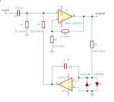
For amplifiers that don't have to noise-match a very low input impedance (no MC headamps), when you want a very flat magnitude response, I can recommend the attached topology. Audiophiles are bound to dislike it: those who dislike coupling capacitors will dislike the coupling capacitor and those who dislike DC bias servos will dislike the entire circuit.
One advantage is that it is a second-order high-pass, so with proper sizing you get a second-order Butterworth response that has much less droop a few octaves above its corner frequency than a first-order filter. Another advantage is that the op-amp only has to handle very small signal currents, and that its output impedance is not a part of the gain setting voltage divider of the main amplifier.
The quality factor will depend on the driving impedance to some extent, but large driving resistances only increase damping a bit. They can't make it peak or oscillate. Small driving capacitances (like a source with an AC coupled output with a relatively low capacitance) shift the corner frequency upwards and increase damping.
The reason why I wouldn't recommend it for MC headamps is the effect of the coupling capacitor on noise when the amplifier has a large equivalent input noise current. JFET-based MC headamps have no large input noise current, so maybe it could work for those.
Attachments
Last edited:
Thanks for the detailed explanation. Everything you say makes sense and is defensible.
...
Thanks again for responding to my question.
I'm too pleased to talk with you!
But there are always tradeoffs and I don't know how to evaluate them. For instance, removing feedback from around the VAS leaves more loop gain for global error correction, but at the cost of increased VAS distortion. The VAS collector is a high-impedance node, but maybe not as high as you think, depending on the Early voltage of the device. Reduced local feedback makes the VAS transfer function more dependent on the transistor's gain variability and nonlinear output capacitance. I can't say how that affects sound quality.
Tradeoffs, of course.
Let's try to evaluate.
First of. VAS output aren't just itself it's coupled and loaded to the OPS input.
In shown example a load resistance of 1k are trasferred to the VAS output by the beta factor of OPS transistors like 500 times. So regardless of Early effect VAS output node will not be too high impedance.
Second of. VAS could be easily built on the transistors with high Early effect and moreover cascoded with base current compensation. We actually can make really high impedance node but the main issue will be not the resistance itself, capacitance and parasitic leaks of such a point dominates in discrete design. Unfortunately just one unwashed fingerprint or homemade board will totally destroy all simulated compensation efforts. Opamp chips are better in terms of very low parasitics named, but most well-known opamps are too much overcompensated.
Referring to the paper you linked earlier, your approach is good for integrated op-amps where you can't get at the internal nodes for compensation. This isn't a constraint for discrete designs. I don't know what the pros and cons are of moving some of the loop compensation to the external feedback network, versus applying it to the forward gain path.
Please, let me again answer more thoroughly.
This isn't just moving pole-zero between stages.
We put in scheme a gain stage, we want a gain from it, correct? As more stable gain as better, isn't it? So why drop out such a gain in a most needed HF region by simple and straightfirward shunting it's load resistance?
First that this approach gives - is a most achievable stabilized gain at high-frequencies, dozens of kHz. Not just by moving pole-zero placement, but by excluding unneded shunting of high impedance nodes. Just leave them loaded to an RC from 3x to 5x times than intrinsic devices parasitics (more valueable - all changing parasitics, like follower input capacitance or changing Cob) and that's more than enough.
All of the papers I've read about two-pole compensation point out the increase in available loop gain for feedback, but don't mention that you're really just reallocating a fixed amount of GBW between local and global loops.
No, this is not only reallocating GBW. Just integrate an area under Bode plot and you can see how much this approach adds to the GBW at a given unity gain bandwidth.
I was reading about Kevin Gilmore's Dynalo amplifier this morning. He is adamant that an amplifier should have low global loop gain, and is dead-set against conventional DC offset servos. All of these arguments seem valid and each design approach has its proponents. It's all very interesting, but inconclusive.
Heh, let's talk about.
First, Kevin claims "no capacitors in feedback loop". That's not clearly so. Say Dynahi. Just check Cob and hFE of the output devices and you'll see how much VAS output loaded by OPS input capacitance and load resistance translated to the OPS input. Yes, he dropdown straight VAS load resistance to a low enough value, but this not only pushes RC-constant of the dominating pole to the ~300 kHz, but also add distortion due to high thermal effects of the changing VAS current. Let's remember first wizard's rule - changing current asks to stable voltage, changing voltage asks for stable current.
About servo it's not so clearly too.
Transistor virtually have two input nodes (base/gate and emitter/source) and one output node (collector/drain), any input can be used to drive output. Patented Kevin's approach allows to use second usually nondriven input to summarize signal and servo signals at the output node.
Your last Bode plot goes deep into the zone of conditional stability. Nyquist is perfectly happy, but as I mentioned above, what are the real-world consequences under large-signal conditions? Is there some mysterious subjective impact of radical shifts in group delay across the frequency spectrum?
Hmmm, hard question.
I have an amp with unprecedently high feedback depth. Rail capacitors are well audible here too. I have no answers.
I know of a fellow who would be happy to show you many, many graphs purporting to prove there is, LOL.
Aaargh, doesn't say his name here, he can hear and came!!!
LOL
I've been in a low energy phase lately, but if I can get the motivation, I may throw your schematic in SPICE and see if I can come to any conclusions of my own.
I have attached basic bones, feel free to add a meat on your choice!View attachment attachment(2).zip
Last edited:
It shouldn't say "diyAudio Member" under your name Pavel, it should say "Preacher of decompensated OpAmps" 😉
I have PCBs on the way for a composite headphone amplifier with THS4021 and a follower OPS with CCS load, so I will be evaluating this approach that you mentioned quite a few times. I am interested to see how it will go. In the same order are PCBs for hpasternack's headphone amplifier and that PCB also seems spacious enough for some modifications should I feel any desire to investigate the compensation aspect further.
I was also thinking about designing a discrete or hybrid OPA with JFET input transistors (but mainly for measurement purposes) so I will keep an eye on this thread as well. I can't open the .asc file in "attachment(2).zip" on my Mac, but I will try on my Windows machine.
Your last Bode plot goes deep into the zone of conditional stability. Nyquist is perfectly happy, but as I mentioned above, what are the real-world consequences under large-signal conditions? Is there some mysterious subjective impact of radical shifts in group delay across the frequency spectrum?
Ah, yes, this is a common thoughts.
Bode graph shows openloop behaviour while being closed there are virtually no any phase impact.
It shouldn't say "diyAudio Member" under your name Pavel, it should say "Preacher of decompensated OpAmps" 😉
Sorry, but we're on the "feedbacked" highway and there are no reversal...
😛ardon:
I have PCBs on the way for a composite headphone amplifier with THS4021 and a follower OPS with CCS load, so I will be evaluating this approach that you mentioned quite a few times. I am interested to see how it will go. In the same order are PCBs for hpasternack's headphone amplifier and that PCB also seems spacious enough for some modifications should I feel any desire to investigate the compensation aspect further.
Feel free to ask and show your results.
I was also thinking about designing a discrete or hybrid OPA with JFET input transistors (but mainly for measurement purposes) so I will keep an eye on this thread as well.
I suppose it's better to create dedicated tread and thoroughly talk about.
I can't open the .asc file in "attachment(2).zip" on my Mac, but I will try on my Windows machine.
Ok, let me know.
There are nothing special and even "Tian probe" from LTspice tutorial files directory can be modified for this.
One advantage is that it is a second-order high-pass, so with proper sizing you get a second-order Butterworth response that has much less droop a few octaves above its corner frequency than a first-order filter. Another advantage is that the op-amp only has to handle very small signal currents, and that its output impedance is not a part of the gain setting voltage divider of the main amplifier.
The quality factor will depend on the driving impedance to some extent, but large driving resistances only increase damping a bit. They can't make it peak or oscillate. Small driving capacitances (like a source with an AC coupled output with a relatively low capacitance) shift the corner frequency upwards and increase damping.
Thank you for the circuit suggestion. I like the fact that you're looking objectively at the filter tuning and designing for maximally-flat response. This is better than just willy-nilly putting in an integrator and declaring it good enough.
I used the servo from the DCG3 (which is bog-standard anyway) and didn't give it further thought. I'm thinking the best solution is probably to leave the servo out entirely and focus on careful design for low offset without any correction whatsoever. Maybe easier said than done. I'm conditioned to avoid coupling capacitors, but practically speaking they are a pretty good solution, if you can cope emotionally.
Hmmm, hard question. I have an amp with unprecedently high feedback depth. Rail capacitors are well audible here too. I have no answers.
I appreciate the effort you've put into developing these ideas. I quoted this one thing because I have to admit I just don't know, either. Back in the day, before I stopped calling myself an audiophile, I used to go to stereo shops to listen to gear I had no intention of buying. I nodded my head appreciatively in response to cues from the salesmen, but honestly rarely heard any difference between amplifiers. I do remember comparing a Muse Model 100 to some Classe amplifier and being struck by the contrast. But I gave up buying commercial gear a long time ago. You would be appalled if you saw my living room system, ugh.
It's only this year, when I got into headphones, that I started thinking about "critical listening" again. So I don't claim any credentials as a subjective evaluator.
I believe what you say about the audibility of capacitors and so on. But I also have to wear my skeptic's hat and remind myself that what you hear is real for you, but might not sound the same to me. I would be making a fool of myself if I tried to add anything deeper than that to the discussion.
What I mean about shuffling gain between local and global loops may be obvious, but I'll restate it differently just for kicks. If the VAS is perfectly linear without feedback, then throwing away gain to linearize it is a waste of loop gain that could be put to good use around the output stage. On the other hand, the local feedback has effects, both beneficial and detrimental, on the impedances looking in and out of both sides of the stage. And if the VAS is adding nonlinearity, it might be advantageous to correct it via a tight local loop. You can throw every trick you know at a circuit (like a Hawksford cascode) and maybe get better performance in a SPICE simulation. But these are second-order effects and, as you say, a fingerprint on the board can undermine everything. Every part you include adds complexity and more variables. Pardon me for stating the obvious as if it's profound.
Anyway, I like your ideas and you've given me more things to think about as I mull my next project.
Hi Greg and Ken, I have packed a pair of blank boards for each of you, included the schematic and a bill of materials with some notes and my off forum contact information if you have questions. I am hoping to mail them this week from the local post office, but will definitely do it after Christmas. Sorry that I am taking so long to get them out to you guys, it's been a busy and bumpy couple of months for us.
These are the last version with two pole compensation.
I appreciate your curiosity and look forward to your feedback, comments and suggestions if I decide to do another iteration.
I'll be building up a pair myself for use in the tape amplifier they were originally designed for.
I use some of the earlier ones as a buffers for older cassette decks that need about 10dB additional gain to match my system design levels (CD red book) and in a simplistic line stage.
This is the PCB for the latest version with two pole compensation. I think I need to wipe down my work surface.. LOL
The left photo is of the input and VAS stages, the diamond buffer output is on the other side as shown on the right. The op-amps are on 4 layer PCB.

The left photo is of the input and VAS stages, the diamond buffer output is on the other side as shown on the right. The op-amps are on 4 layer PCB.

- Home
- Source & Line
- Analog Line Level
- Playing at Discrete Op-Amp Design