Hey All,
I've made some significant progress in my project to convert my Pioneer PD-91 CD Player to a DAC. I wanted to provide an update on it as well as seek some guidance on an issue I'm having.
(Background: the laser died and I decided to convert the player to a DAC. I am not super experienced with this level of modification, so this has been a learning curve for me).
What has been done:
Any help would be greatly appreciated!😀😉
I've made some significant progress in my project to convert my Pioneer PD-91 CD Player to a DAC. I wanted to provide an update on it as well as seek some guidance on an issue I'm having.
(Background: the laser died and I decided to convert the player to a DAC. I am not super experienced with this level of modification, so this has been a learning curve for me).
What has been done:
- I installed a digital interface board which utilizes a Burr Brown DIR9001 chip - this seemed like a relatively smart choice because it is easy configurable for 384fs
- The digi-interface is routed into the player via the digital filter (Yamaha YM3414) - I felt that going into the Pioneer's filter will retain as much of the original sound character.
- I have attached the following PDF where you can see how I've connected the components: View attachment DIR9001 Connections to Yamaha YM3414.pdf
- With all data and clock connections (refer above PDF) I have cut the corresponding trace connections on the Pioneer's PCB. This was to ensure the digital filter is only being fed data and clock from the DIR9001.
- In order to prevent the player muting it's output stage, I have severed the internal 'Audio Muting' function. I have attached a PDF showing where I have made this cut: View attachment Muting Cut.pdf . The Schematics show the yellow highlighted goes all the way to the output stage.
- I am fairly confident it was the correct method to disable muting by simply cutting this trace because according to the table here: View attachment Muting Cut 2.pdf it would appear if there is no voltage coming from this pin that the analog output would not be muted.
- The modification works (!), if I play music through the DIR9001 (either SPDIF or USB) the Pioneer output produces music - great sign.
- It doesn't appear to have any noticeable jitter or drop-outs.
- However the volume is very low 🙁 If I were to estimate, I would say that the output volume is about 50db lower than it should be.
- I have been doing a lot of troubleshooting and thinking about this over the last 2 weeks and I am not getting any clarity on why the output level is so low.
- My first theory was that somehow the cut I made to the muting circuit wasn't effective. So I made a secondary cut, much closer to where the muting circuit is on the output stage. This made no difference.
- I then thought that the player's internal 'digital attenuation' IC may be doing something, however, this would make no sense because as far as I can tell from the Schematics the attenuation is applied directly to the data stream as it enters the digital filter, but as I have cut that connection and the digital filter only sees the DIR9001, there should be no form of attenuation applied.
Any help would be greatly appreciated!😀😉
Last edited by a moderator:
Do the formats match ? They should both be right justified 16 bit data as per the top of fig 15 of the DIR9001 datasheet.
Last edited:
Ah! See the problem. The YM3414 is an 18bit filter. Left justified data wouldn't matter but with 16 bit right justified data you have to pad with two bits or the MSB is in the wrong place.
Ah! See the problem. The YM3414 is an 18bit filter. Left justified data wouldn't matter but with 16 bit right justified data you have to pad with two bits or the MSB is in the wrong place.
Many thanks for the response rfbrw! Always very helpful.
The 16bit vs 18bit issue is something I hadn't considered (this is where my inexperience with digital audio will really show). My expectation was that the word length entering the filter was always going to be 16bit and somehow the additional 2bits were specific to a function of the filter. However if the filter expects to receive 18bits length, this must be problematic...
- Given the above, my expectation would be that if the filter expects to see 18bits depth, and only receives 16bit, this would cause something like a 15db drop in signal - is that right? However, as I said, I'm seeing something close to 50db - would this be to do with the incorrect placement of the MSB?
- I understand the concept of a decimation filter, but I wouldn't know where to start with 'padding' an additional 2 bits??
- The DIR9001 is capable of 24bit output, would it potentially be easier to truncate that output down to 18bit? Given that the audio it will be receiving is only 16bit 44.1khz, I don't see there being any issues with dithering?
Last edited by a moderator:
If you can measure the signal level at the output of the dac chip then one can have a better idea where the problem is. If you use a signal generator program such as ARTA or REW, you could feed the dac a 0dBFS, 1kHz (or other frequency) digital test signal. If the voltage level out of the dac chip is 2-3v peak to peak (or maybe even a little less) that would seem reasonable. The problem would then probably be after the dac chip. If the signal level is too low at the dac chip output then I would look for a problem on the digital side before the dac chip. A scope can be helpful if one is available.
Last edited:
Many thanks for the response rfbrw! Always very helpful.
The 16bit vs 18bit issue is something I hadn't considered (this is where my inexperience with digital audio will really show). My expectation was that the word length entering the filter was always going to be 16bit and somehow the additional 2bits were specific to a function of the filter. However if the filter expects to receive 18bits length, this must be problematic...
Looking forward to your feedback!🙂
- Given the above, my expectation would be that if the filter expects to see 18bits depth, and only receives 16bit, this would cause something like a 15db drop in signal - is that right? However, as I said, I'm seeing something close to 50db - would this be to do with the incorrect placement of the MSB?
- I understand the concept of a decimation filter, but I wouldn't know where to start with 'padding' an additional 2 bits??
- The DIR9001 is capable of 24bit output, would it potentially be easier to truncate that output down to 18bit? Given that the audio it will be receiving is only 16bit 44.1khz, I don't see there being any issues with dithering?
The MSB is the sign bit. It signifies to all whether the word is positive or negative. With right justified data its position moves relative to word length so the dac or filter has be implicitly set for that wordlength otherwise it is like being due a £1000 only for someone to move the decimal point two places in the wrong direction and you are left with a tenner.

Try this.
Many thanks rfbrw! This is very helpful.
Based on your diagram and feedback, my understand is this:
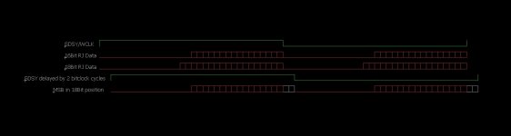
You suggest delaying the Left-Right Clock by the equivalent of 2 bit cycles, to allow the MSB of the 16bit word length to arrive at the same time as the YM-3414 would expect the MSB of a 18bit word length. Is that a correct summary?
Some short questions:
- Why have you suggested using two D flip-flops and not one?
- I calculate each bit cycle to be 354.31ns long, so I will need a total of 708.62ns delay is total - does that sound about right?
Yes.
One flip flop, one cycle. If you look at some of the NOS dacs where one channel has to aligned with the other, you'll see a much longer chain of flip flops.
Don't bother too much about the actual time. SDSY, DATA and BCLK are all in sync so all that matters is the delay relative to each other.
One flip flop, one cycle. If you look at some of the NOS dacs where one channel has to aligned with the other, you'll see a much longer chain of flip flops.
Don't bother too much about the actual time. SDSY, DATA and BCLK are all in sync so all that matters is the delay relative to each other.
Yes.
One flip flop, one cycle. If you look at some of the NOS dacs where one channel has to aligned with the other, you'll see a much longer chain of flip flops.
Don't bother too much about the actual time. SDSY, DATA and BCLK are all in sync so all that matters is the delay relative to each other.
Brilliant!
So essentially each Flip-flop is configured to be triggered by the instance of a 1bit cycle in the bit-clock, therefore, by having 2 of them 'daisy-chained' the LRCLK should be delayed exactly the 2 cycles.
I was thinking that a single flip-flop would be regulated to provide an approximate 2 cycle delay (as I said around 708ns) but this makes more sense.
I get what you're saying about everything being relative.
You could build a circuit that will hold high or low for a given period but you would loose the clocking action.. It would just hold steady for 2 cycles.
You could build a circuit that will hold high or low for a given period but you would loose the clocking action.. It would just hold steady for 2 cycles.
Your proposed implementation seems really logical. I'm going to pick up a pair of 74HC74Ns and give it a go.
Update soon!
Try this.
Hey rfbrw!
Just an update and question.
I am in the middle of putting together a PCB design in KiCAD for this flip flop delay.
I noticed that in your suggested schematic you had power/GND connected to pins 1 and 4, as well as 13 and 10.
Reading the technical specs for 74HC74, it seems that Vcc is pin 14 and GND is pin 7. It suggests that all unused inputs are set to GND and all unused outputs to Vcc. I assume this is why you have it done it the way you did?
See attached a copy of a schematic I've put together (

) , do you see any issues with that? Or do you think pins 1 and 4 should be grounded and 13 and 10 Vcc?
Last edited by a moderator:
1,4,10 and 13 are all active LOW. Pulling them to ground turns them on. Since the are not needed pulling them high turns them off. The unused outputs can float.
Hey All/ @rfbrw
An update on progress / further advice needed:
I've received the PCB that I had printed and after soldering the ICs, etc. have installed it into the Pioneer (forgive the shocking job I've done, my experience with SMDs is minimal)..

Unfortunately, it doesn't appear to work and the Pioneer isn't receiving any signal from the SPDIF source. I've yet to do in-depth troubleshooting but considering the less-than-ideal job I've done with soldering it could be something went wrong there.
Alternatively, perhaps something is wrong with the design. @rfbrw / others - do you see anything wrong with this:

Cheers,
Fish
An update on progress / further advice needed:
I've received the PCB that I had printed and after soldering the ICs, etc. have installed it into the Pioneer (forgive the shocking job I've done, my experience with SMDs is minimal)..
Unfortunately, it doesn't appear to work and the Pioneer isn't receiving any signal from the SPDIF source. I've yet to do in-depth troubleshooting but considering the less-than-ideal job I've done with soldering it could be something went wrong there.
Alternatively, perhaps something is wrong with the design. @rfbrw / others - do you see anything wrong with this:
Cheers,
Fish
tie both grounds J1 and J2 should to psu gnd (node that feeds Inv_1 pin7, FF_1 pin7).
tie the five unused inputs on Inv_1 to pin 1 or pin 14.
tie the five unused inputs on Inv_1 to pin 1 or pin 14.
The five unused inverter inputs have to be connected to either supply or ground, like tincanear wrote. The connector grounds should be connected to the inverter and flip-flop ground pins without large detours (maybe that's already the case if there is a ground plane) and there should be power supply decoupling capacitors (100 nF ceramic X7R, for example) between supply and ground, close to each IC.
On top of that, you have shorted the inverted flip-flop outputs to ground. Unused outputs should be left open.
On top of that, you have shorted the inverted flip-flop outputs to ground. Unused outputs should be left open.
I would also bring out each pin to a via instead of routing direct from one pin to another under the chip. makes it easier to modify the circuit (if original design doesn't work exactly as planned). +1 to the bypass from gnd to +Vcc on each IC. instead of using a hex inverter, there are some tiny logic parts that feature one or two gates in a smaller package (e.g. single nand in 5-pin SOT-23-5 package)
re-reading the thread, it appears that the OP has fabricated PCB & soldered parts to it. in that case, easiest fix is to desolder the unused output pins 6 and 8 of the flip-flop and lift them into the air a mm or two above the traces with an exacto knife or similar tool. shorting those outputs to ground may have destroyed the flip flop (or not, depending on how long power was applied), in which case pcb traces to flip flop pins 6 and 8 can be cut after removing damaged chip. leaded mono ceramic bypass caps, 1 per chip, can be tack soldered to pins 7 and 14, keeping lead wires as short as possible.
also make sure that chassis mounting frame (copper plated???) does not short underside of the pins for J1 or J2.
also make sure that chassis mounting frame (copper plated???) does not short underside of the pins for J1 or J2.
Last edited:
- Home
- Source & Line
- Digital Source
- Pioneer PD-91 DAC Conversion Update and ASSISTANCE(!)