re-reading the thread, it appears that the OP has fabricated PCB & soldered parts to it. in that case, easiest fix is to desolder the unused output pins 6 and 8 of the flip-flop and lift them into the air a mm or two above the traces with an exacto knife or similar tool. shorting those outputs to ground may have destroyed the flip flop (or not, depending on how long power was applied), in which case pcb traces to flip flop pins 6 and 8 can be cut after removing damaged chip. leaded mono ceramic bypass caps, 1 per chip, can be tack soldered to pins 7 and 14, keeping lead wires as short as possible.
also make sure that chassis mounting frame (copper plated???) does not short underside of the pins for J1 or J2.
Hey Both - thank you very much for your helpful feedback 👍The five unused inverter inputs have to be connected to either supply or ground, like tincanear wrote. The connector grounds should be connected to the inverter and flip-flop ground pins without large detours (maybe that's already the case if there is a ground plane) and there should be power supply decoupling capacitors (100 nF ceramic X7R, for example) between supply and ground, close to each IC.
On top of that, you have shorted the inverted flip-flop outputs to ground. Unused outputs should be left open.
Based on what you've said, I'm going to draw and print a new PCB , a "v2" prototype.
Just summarizing/confirming your suggestions before I go and make changes in KiCad:
- Connect the GNDs from J1 and J2 to the same GND as used for the ICs
- Tie all unused input pins of the Inverter (pins 3,5,7,11,13) to the 5V supply (pin 14)
- Place a decoupling capacitor between the 5v supply and ground for both ICs (near to ICs)
- Leave the unused outputs of the flip flop (pin 6 and 8) open (un-traced pads)
- Bring all traces that are currently routed under the ICs to a Via instead, as to use the 2nd layer of the PCB to trace between pins on the same IC
@MarcelvdG , the only point I didn't understand is when you said:
Could you clarify that one?On top of that, you have shorted the inverted flip-flop outputs to ground.
@tincanear, regarding your suggestion for the SOT-23-5, I have heaps of these 74HC inverters and Flipflops, I'll stick with using them until I've finished prototyping and get a working solution, will look at perfecting everything for v3! 😉
You covered it with your point 4. Pins 6 and 8 were connected to ground, and pins 6 and 8 are the inverted outputs of a 74HC74. The 74HC74 tries to drive them high whenever a low level is clocked into the corresponding flip-flop. That's the inverse of pins 5 and 9, the 74HC74 tries to drive those high when a high level is clocked into the corresponding flip-flop.
recommendations:
0127a. Make all GND and +5V VCC traces a lot (perhaps 5x or 10x) wider.
0127b. tie all unused inverter inputs to Vcc each through a separate 0805 SMT resistor (any value between 100 ohms and 3k should work just fine)
0127c: bring all unused inverter outputs to a pad or via
you can post v2 layout here before fabricating
Tincanear, is that because you want to be able to use the unused inverters when something unexpected happens?
You covered it with your point 4. Pins 6 and 8 were connected to ground, and pins 6 and 8 are the inverted outputs of a 74HC74. The 74HC74 tries to drive them high whenever a low level is clocked into the corresponding flip-flop. That's the inverse of pins 5 and 9, the 74HC74 tries to drive those high when a high level is clocked into the corresponding flip-flop.
Thanks Both!recommendations:
0127a. Make all GND and +5V VCC traces a lot (perhaps 5x or 10x) wider.
0127b. tie all unused inverter inputs to Vcc each through a separate 0805 SMT resistor (any value between 100 ohms and 3k should work just fine)
0127c: bring all unused inverter outputs to a pad or via
you can post v2 layout here before fabricating
Going to jump on KiCad over the next few days. Hopefully have a V2 ready by the end of this week.
@tincanear & @MarcelvdG @rfbrw
Better late than never (!) - sorry for the slow update on this, life got in the way in the last 6 months.
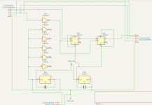
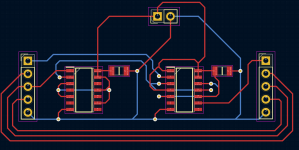
I finally got around to drafting the revised PCB in Kicad. Would be very pleased for any feedback at all!


Better late than never (!) - sorry for the slow update on this, life got in the way in the last 6 months.
I finally got around to drafting the revised PCB in Kicad. Would be very pleased for any feedback at all!


If not, and
Edit: I just looked up what PWR_FLAGs are for and it's just a directive for the ERC, not a connection by label. No problem!
Last edited:
Many thanks Marcel.I'm not familiar with those PWR_FLAG devices. Do they short supply to ground via label? I don't see any such short in the layout, but ground fill might short supply and ground if those PWR_FLAG devices cause them to have the same net name.if you have the pin order of the connectors correct, then I think this should work, even though you haven't implemented tincanear's recommendations from post #23. Most of those are only meant to make tweaking it easier if anything goes wrong.
If not, and
Edit: I just looked up what PWR_FLAGs are for and it's just a directive for the ERC, not a connection by label. No problem!
I'm going to try an implement those additional suggestions by Tincanear before printing the next PCB.
Will keep everyone posted on progress
- Home
- Source & Line
- Digital Source
- Pioneer PD-91 DAC Conversion Update and ASSISTANCE(!)