There are many Ceramic multilayer 1 uF 0805 caps available, at least when looking at Farnells website.I knew I'd mess up somewhere with this... I double checked the schematic against the simulation in TinaTI and hit the order button with pcbway. Then when ordering the components realised I'd specced 1uF 0805 SMDs in the sub-sonic filter. As far as I can tell these don't exist as C0G NP0 types so I'm trying to work out an alternative.
I'm resigned to the fact I need to correct the design for a permanent solution but in the mean time is there a capacitor (even a leaded type) that I could use to test? Ideally lowest thd and minimum tolerance in that order of importance.
Any ideas would be great.
They may not be what you had in mind, but they will do the job without a doubt.
Hans
Thanks, I think you're right... any preference for X7R or X8L, I realise this is going to be sub-optimal anyway.
This polyester baby has a lead spacing of 2.5mm, fits on 0805 pads.
Available from Farnell.
http://www.farnell.com/datasheets/1...MIsYGeqOSM2QIVa7XtCh0jKA9_EAAYAiAAEgJiiPD_BwE
MKS0B041000F00KSSD -The link doesn't work for me, do you have the component number, I can look that up.
Thanks.
Film Capacitor, 1 µF, 50 V, PET (Polyester), ± 10%, MKS0 Series
I'd specced 1uF 0805 SMDs in the sub-sonic filter
As far as I can tell these don't exist as C0G NP0 types
You can stack 2 or 3 smaller value caps of the same footprint easily enough.
Thanks, that looks like a good option... I'd been looking at some monster polypropylene caps - they were going to look a bit precarious on those 0805 pads.MKS0B041000F00KSSD -
Film Capacitor, 1 µF, 50 V, PET (Polyester), ± 10%, MKS0 Series
That's an interesting idea... I can get NP0 C0G up to 470n and 5%, a pair of those will get me close. I'll try to adjust the resistor values to make that work.You can stack 2 or 3 smaller value caps of the same footprint easily enough.
Thanks for the ideas.
I can get NP0 C0G up to 470n and 5%, a pair of those will get me close.
I'll try to adjust the resistor values to make that work.
Stacking SMT parts works very well, and I've done it many times.
Solder one end at a time, and allow to cool before soldering the other end.
The COG/NPO types are excellent, much better than mylar/polyester types.
Last edited:
I can get NP0 C0G up to 470n
Must test my glasses, I thought there was an extra 0 on the capacitance in pF... looks like 47n is the max value through Farnell - don't think I'll be able to stack 20 of them! Nice idea to stack them though... I'm sure that will come in handy in future.
I think I had a brain fart when I specced the ceramics, looks like I'll be using the stacking technique sooner than I thought. The 6n8 is now a stack of 4n7, 1n8 & 300p and the 5n6 is a stack of 2*2n2 and a 1n2.
The parts bill is a shocker - £265 and I had a few of the parts in the spares bin. Mostly down to the NP0 ceramics and minimum order quantities.
I think a bit of cost optimisation before version two!
The parts bill is a shocker - £265 and I had a few of the parts in the spares bin. Mostly down to the NP0 ceramics and minimum order quantities.
I think a bit of cost optimisation before version two!
Schematic readability:
I am well retired from all this, but I do have a bee in my bonnet about this aspect of electronic schematics!
A schematic should first of all be readable to explain the operation of the circuit. It does not need to relate to physical topology of the components.
All my experience was with Orcad which allowed separation of different parts of the component onto separate parts of the schematic - even (and sometimes preferably) onto separate sheets.
As an illustration, remove all relay coils from their contacts. Coils and their drivers, diodes etc can be drawn in the most logical digital fashion. The contacts can then be a simple primitive "switch" component in the optimum place on the normal analog diagram.
I don't know if your schematic editor can do this, but I would not use it if it couldn't!
Edit: The schematic is not needed to build the product, only the BOM and layout. The schematic is for the poor old field engineer so s(he) can understand it and fix it decades after the product was produced.
Best ever schematic and general drawing practice was Tektronix analog scopes - but I'm an old f-r-
Last edited:
If you can send me a BOM with prices, I can suggest where cost reductions can be made.I think I had a brain fart when I specced the ceramics, looks like I'll be using the stacking technique sooner than I thought. The 6n8 is now a stack of 4n7, 1n8 & 300p and the 5n6 is a stack of 2*2n2 and a 1n2.
The parts bill is a shocker - £265 and I had a few of the parts in the spares bin. Mostly down to the NP0 ceramics and minimum order quantities.
I think a bit of cost optimisation before version two!
Hans
The parts bill is a shocker - £265 and I had a few of the parts in the spares bin.
Mostly down to the NP0 ceramics and minimum order quantities.
Perhaps a different SMT size will be more available and cheaper, though NPO/COG types are
always more expensive. The 1206 is easier to mount, also.
Schematic readability:
A schematic should first of all be readable to explain the operation of the circuit. It does not need to relate to physical topology of the components.
I totally agree... I'm an amateur and I'm learning how to do this. Luckily I'm the only field engineer who's likely to deal with this so I'll only have myself to blame!I don't know if your schematic editor can do this, but I would not use it if it couldn't!
I'm using Eagle software and I've not found a way of splitting the physical components into their constituent parts to simplify the schematic. There may well be a way of doing this that I've not discovered or perhaps at some point I'll need to learn some software that can.
Thanks, I'll send you what I have... I don't mind spending the money, the spare components will get used sooner or later. But if I can reduce the cost that would be useful.If you can send me a BOM with prices, I can suggest where cost reductions can be made.
Hans
I didn't consider cost when designing, it's a good lesson. I'll have a look at the other options with the next design.Perhaps a different SMT size will be more available and cheaper, though NPO/COG types are
always more expensive. The 1206 is easier to mount, also.
Looking at this again a lot of the cost was in the minimum order quantity of components (10x / 25x) so future iterations shouldn't cost as much. The other major cost is stacking up NP0/C0G to make the 100n caps in the servo I'm not sure how critical the values are or how much they contribute to thd/noise as they'll have little voltage across them in the audio FR. If I can use 5% X7R or similar for these I'll be saving myself £40 straight off - perhaps I'll try that first and change them later.
I guess I'll treat this one as a learning exercise.
Also I've just discovered how to build components in Eagle using one footprint and multiple schematic symbols... that should help me simplify things.
I guess I'll treat this one as a learning exercise.
Also I've just discovered how to build components in Eagle using one footprint and multiple schematic symbols... that should help me simplify things.
Last edited:
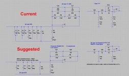
Image below shows what I suggest, including some Farnell part numbers.
On top of that, you have used Omron relays the G6SK series.
From TE Connectivity there is the IM series. Their footprint is much smaller, cost is almost 50% lower and they are very reliable.
Hans
On top of that, you have used Omron relays the G6SK series.
From TE Connectivity there is the IM series. Their footprint is much smaller, cost is almost 50% lower and they are very reliable.
Hans
Attachments
Thanks for the suggestions Hans, I had more or less completed a re-design so I've gone with some of the original values. The reason I was looking for NP0 for the Servo was because I made a mistake and made them 0805 on the layout. I've now decided to get the boards re-made rather than botch the job.
I decided to go with polypropylene for the larger caps in the end. They're a bit big but don't impact the layout too much.
I've learned a lot about Eagle doing this so it doesn't feel like wasted effort. Having read a bit about using curved traces I'm not convinced they'll make any difference to performance, but they look nice so I've used them.
The only thing I can't decide on now is whether to include the orphans in the pours, or to remove them and leave large voids. I'm tending towards the first option.
I could only find latching relays in the TE range with a single coil - which would have meant quite a few H-bridges. I think the main impact on component cost was trying to use larger value NP0s.
Hopefully the schematic is now much improved too.
Thanks again for all the help.
Simon
Attachments
BOM is now a bit more reasonable, I need to spend £130 to get the parts (because of minimum quantities), which works out as £82 including VAT per board.
Also I spotted a couple of errors in the schematic, I forgot the 68k across the output and the RIAA has a 31k which should be 9.31k.
Also I spotted a couple of errors in the schematic, I forgot the 68k across the output and the RIAA has a 31k which should be 9.31k.
- Status
- This old topic is closed. If you want to reopen this topic, contact a moderator using the "Report Post" button.
- Home
- Source & Line
- Analogue Source
- Phono Stage PCB Layout