I'm working on a PL700b for a friend. As the title says, its completely original and currently working fine. My friend wants it gone through completely as well as having it converted from the original quasi complementary output stage to a full complementary output. Before getting started I've done a lot of research on this amp. I've found quite a bit of info on what to do in the way of upgrading it, but the conversion info is spotty.
My big concern is that I perform the quasi to full comp conversion properly. I've redrawn the original schematic for the PL20 control pcb to show the planned changes for the conversion. I'm hoping there is someone familiar with these amps that can tell me if I'm on the right track or if I've missed something.
I've attached the original and modified drawings. Any info would be appreciated.
Looking at your redrawn schematic, you are on the right path;
- Remove R23, R34, R35, D13 and C18.
- Remove R41, 0.33 collector resistor (Protection circuit)
- Install jumper where R23 was.
- Where you have indicated to "cut trace", this wire and can be rerouted and connected to B- for Q7 collector negative power supply.
- A new wire needs to be connected from the emitter of Q7 to the base of Q12. This is your negative base drive.
- "Base Stopper" resistors would be a good idea to insert between Q7/Q10 and Q11/Q12
To rewire the output stage transistor sockets, you can use solid copper 18 gauge wire from Home Depot/Lowes and strip off the insulation. This wire will bend and solder easily.
I'll upload some pictures of the 400II output stage I modified later (Not at home now).
"Some people actually prefer the older discrete design over the later IC op-amp design "
Comparing the Flame 400 discrete board with the Flame 400 with the newer IC board, the newer board won hands down.
Amps were used on horn-loaded MF and HF (in a tri-amped PA), and the IC ones sounded much, much cleaner.
I'm sure it would have been better with a better opamp, the LF351 has room for improvement.
YMMV.
Last edited:
Take a look at white oak audio for their driver board replacement..... cures the instability problems.
I predict we will cover every subject under the sun before Chamberman gets his 700B converted to full comp...
Yes, I am feeling pugnacious today.
Yes, I am feeling pugnacious today.
Looking at your redrawn schematic, you are on the right path;
- Remove R23, R34, R35, D13 and C18.
- Remove R41, 0.33 collector resistor (Protection circuit)
- Install jumper where R23 was.
- Where you have indicated to "cut trace", this wire and can be rerouted and connected to B- for Q7 collector negative power supply.
- A new wire needs to be connected from the emitter of Q7 to the base of Q12. This is your negative base drive.
- "Base Stopper" resistors would be a good idea to insert between Q7/Q10 and Q11/Q12
To rewire the output stage transistor sockets, you can use solid copper 18 gauge wire from Home Depot/Lowes and strip off the insulation. This wire will bend and solder easily.
I'll upload some pictures of the 400II output stage I modified later (Not at home now).
Chamberman - If you tell me where you are or what additional information you need for your full comp conversion, I'll be glad to assist.
Attachments

Last edited:
I was thinking that seemed like a bargain for the spaghetti of hard wiring that had to be dealt with in these old 70's amplifiers.
Speaking of spaghetti... I acquired a PL D-500 years ago and have been tinkering with it on and off. It has an oscillation in both channels, which eventually, I will get rid of, but I only throw it some love from time to time. It is way more power than I will ever need, but I have fun tinkering with it. I even thought of converting it to full comp just for the sake of doing it.
In the end, somebody will buy it since they are so rare.
Last edited:
Phoenix Audio Community Forums
You should talk to these guys because they have been doing this for a long time.
They are Phase Linear fanatics, builders, experts, and lovers of all things Phase Linear. Nobody is more devoted to Phase Linear.
You should talk to these guys because they have been doing this for a long time.
They are Phase Linear fanatics, builders, experts, and lovers of all things Phase Linear. Nobody is more devoted to Phase Linear.
Phoenix Audio Community Forums
You should talk to these guys because they have been doing this for a long time.
They are Phase Linear fanatics, builders, experts, and lovers of all things Phase Linear. Nobody is more devoted to Phase Linear.
Maybe Chamberman did. I don't know. He PM'd me and asked if I would give him some advice.
I've done a few full comp conversions with the original driver board. From what i can recall, I didn't cut any tracks on the board. Instead I installed Q7 backwards.
THD+N, Thanks for following up on the specifics of the conversion and looking over my doctored schematic. I looked at what you said about cutting the trace and I thought yeah that makes sense. Then I started wondering why I decided to cut the trace. I realized that when I started doctoring the schematic I started seeing it on my laptop as one big board, output stage and all. I completely forgot that it was a control pcb wired to a back plane when I was deleting components and modifying traces. Looking at what D3IMLAYsays about rotating Q7 looks like it might minimize the work, I'll be installing new transistors at Q7/Q10 anyway so I might as well install Q7 backwards. Then when I pull R34 I can run a wire from the emitter straight to B- using the vacant R34 hole in the board.
You are right, I will be bringing up some other topics about this to hash out with everyone. I have a few ideas already, but I'll save them for now.
To answer your question on where I'm at in the process. I'm still in parts gathering/planning mode right now. I have the wattsabundant relay protect board on order. I bought a set of 24k uF/110V main caps and a new 50A bridge for the power supply. I started working on the PL20 control pcb as well. As I said early in the thread I'm going to do a lot of the upgrade work to the control pcb to begin with while the amp is still a quasi. I am going to be buying a White Oak PL700 replacement chassis as the one this amplifier is in is bent pretty badly to one side. The WO chassis are currently out of stock but should be available later this week some time. Once I have the chassis I'll place one big parts order with Mouser for all of the remaining parts. Then the BIG work will begin.
Here's a question for you, do you think that new TO-3 sockets should be used? I'll be stripping the chassis all the way down anyway. I can get the original TO-3's from digikey for about $1.80 each. Or I could go to a gold plated TO-3 socket off of the bay for maybe $1 each.
BigE We have also investigated the White Oak boards and we are going to hold off on them for now. The goal right now is to see what we can get out of it by refurbing and modernizing it. I told my friend that if he wanted to go that route in the future I could remove the refurbed PL20 control pcb and install the WO control pcb. It wouldn't really be a lot of work at that point.
Audiostar, I have looked over the threads there at Phoenix but I have yet to post there. I also looked over a bunch of the PL threads at Audiokarma.
Last edited:
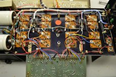
I did a bit more work on this 700b control pcb this weekend. The Q1/Q2 TIS97 input diff pairs were replaced with some matched MPSA18's. The second diff pairs Q3 TIS93's & Q4 MPSA93's were replaced with matched pairs of MPSA92's. A couple of the Q1/Q2 TIS97's hfe had drifted badly, the 4 of them measured 610, 600, 520, 350 on my meter. I also installed the degeneration resistors on the Q1/Q2 diff pair and the back to back diodes across C6 to eliminate the possibility of latching up to one of the rails. I've replaced a number of the front end resistors with Dale RN's as well.
I took DC offset readings before changing the diff pairs out and the offset for both channels was close to zero or so I thought. I kept getting blips of higher voltage when I was measuring it from the speaker posts and then it would drop to zero. It finally seemed stable at near zero on both channels so I went with it. After I changed the Q1/Q2 and Q3/Q4 diff pairs I checked the DC offset again and it started out zero, but once again getting blips of higher voltage. I inspected the binding posts and they are nearly black from 40 years of oxidation. As it turns out I was getting basically no connection by putting my probes into the speaker posts. So I do not know for sure what the pre change out DC offset readings were. I started measuring offset from inside of the amp to get reliable readings. After changing the diff pairs I now have 39mV and 45mV on the two channels. Not horrible, but a little high.
I'm wondering what the reasoning was behind PL using the mixed pairing of TIS93(2N5401) and MPSA93 for the second diff pair Q3/Q4 for the PL20 control pcb. These two have quite different hfe readings, the TIS93's both measure about double the hfe of the MPSA93's. In addition PL had installed a heat sink only on Q4 the MPSA93's. It seems like this mixed pairing almost guarantees DC offset issues or were they trying to cure a nagging offset issue in production by using this mixed pair? Ideas?
Anyway, the amp is working great. No thump at turn on, or turn off and it is silent when powered on without a signal. No signs of oscillation either on the scope or heating of the output zoebel. In addition, it sounds great when playing music, so all is progressing well.
I'm wondering what the reasoning was behind PL using the mixed pairing of TIS93(2N5401) and MPSA93 for the second diff pair Q3/Q4 for the PL20 control pcb. These two have quite different hfe readings, the TIS93's both measure about double the hfe of the MPSA93's. In addition PL had installed a heat sink only on Q4 the MPSA93's. It seems like this mixed pairing almost guarantees DC offset issues or were they trying to cure a nagging offset issue in production by using this mixed pair? Ideas?
The second diff pair is more of a "level shifter" to reference the VAS to the negative supply rail. Q3 / 2N5401 does not need a heat sink because the power dissipation of it is much less than Q4 / MPSA93 because Q3's collector is referenced to ground and not the negative supply rail as is Q4.
I think you will find that Q1 / Q2 will have the most influence on DC off-set, while other circuit parameters will have less influence, but still contribute to it overall.
I have an 700B in very good shape that worked perfectly when i bought it off ebay. Upgrades:
1. Replaced Q3/2N5401 with an MPSA92.
2. Replace Q4 with an MPSA92 as well. I did not bother to match Q3 and Q4.
3. Replaced C6, C11, C15, C16, C22 and C23.
4. Replaced C1, C7 and C10 with silver mica caps.
5. Replaced VU meter and name plate lamps.
I also replaced the original Q1/Q2 with matched pairs of 2N5172's and my DC off-set after warmup is -2.5mV left / -6mV right.
Last edited:
The second diff pair is more of a "level shifter" to reference the VAS to the negative supply rail.
Other designs solve that problem by cascoding that transistor so the 2nd diff pair is more balanced. Even if the transistors are matched, the pair will only really remain in balance if the operating conditions for the pair are the same.
Hmmm, I had a couple of seemingly tightly matched MPSA's for Q1 & 2. Well as tight as my $10 cheapie meter that I use for hfe measurements could read. I might try swapping Q1 and Q2 around in one channel and see if the DC offset changes with the swap. That should at least tell me if that is the issue.
I remeasured my 700B after a considerable warm-up period and it seemed to stabilize around -16mV left / -14mV right.
I still consider this low (enough) and acceptable.
I still consider this low (enough) and acceptable.
VCE of 2N5401 is 150V. VCE of MPSA92 is 300. There's a service bulletin in the manual about 2N5401.
Perhaps in a few months (when the Florida summer forces me to stay inside... I hate the heat and humidity anymore), I'll design a new PL-20 driver board using a standard differential input pair w/ current mirrors, VAS w/ CCS, etc that can be coupled to the original OPS. If this happens, it would be the PCB only. No stuffed boards.
I've been wanting to do this for awhile, but always get distracted by other hobbies (I have too many).
Yes, I know there is already another PL PCB out there... but I'd like to do one based on my ideas.
I've been wanting to do this for awhile, but always get distracted by other hobbies (I have too many).
Yes, I know there is already another PL PCB out there... but I'd like to do one based on my ideas.
Perhaps in a few months (when the Florida summer forces me to stay inside... I hate the heat and humidity anymore), I'll design a new PL-20 driver board using a standard differential input pair w/ current mirrors, VAS w/ CCS, etc that can be coupled to the original OPS. If this happens, it would be the PCB only. No stuffed boards.
I've been wanting to do this for awhile, but always get distracted by other hobbies (I have too many).
Yes, I know there is already another PL PCB out there... but I'd like to do one based on my ideas.
THD+N
Count me in for one if you decide to design and make a small prod run of pcb's. I'll add it to my pile of distractions. 😀
I would be surprised if you couldn't find 25 - 30 diyer's that would be interested in a modernized blank control pcb for their classic PL amp.
I decided to jump out the 300 ohm Q1/Q2 degeneration resistors that I added to see what effect this had on the offset. Doing this dropped the DC offset from the previous readings of -45mv and -39mv to a much more reasonable -15mv & -14mv. While I was doing this I was thinking why not install a 500 ohm pot with the wiper attached to R6 in the tail and the other sides of the pot attached to the Q1/Q2 emitters. Set it to the middle position and use that to trim the degen resistance and adjust the mild DC offset.
Any problems with doing it this way?
Any problems with doing it this way?
I decided to jump out the 300 ohm Q1/Q2 degeneration resistors that I added to see what effect this had on the offset. Doing this dropped the DC offset from the previous readings of -45mv and -39mv to a much more reasonable -15mv & -14mv. While I was doing this I was thinking why not install a 500 ohm pot with the wiper attached to R6 in the tail and the other sides of the pot attached to the Q1/Q2 emitters. Set it to the middle position and use that to trim the degen resistance and adjust the mild DC offset.
Any problems with doing it this way?
Who knows what references were available for power amp design back in the early 70's. I'm sure some guys (Old timers, which I say with great respect and admiration) on this forum knew the challenges back then. Some designs use a trim-pot, and you could certainly try, but DC-offset in the teens is acceptable in my book.
If the original 700B design is kept, with upgraded parts in the obvious locations, the 700B is capable of reproducing music quite well. I would "restore" the amp with only upgraded parts now (don't change the design - yet), then listen to it for awhile and form an opinion. I think you are trying to do too much too fast with all the modifications you initially wanted to do.
I modified an original 400 in the following manner (and it seems to be running and sounding great. Measurements have confirmed it is stable and distortion is very low):
1. Changed the output stage from a triple Darlington to a standard emitter follower full comp stage.
2. Deleted the RCA410 driver transistors.
3. Rewired RCA410 driver transistor sockets to accept another output device.
4. Outputs - MJ15024/25, drivers - 2SA1306B/2SC3298B (Just happen to have a bunch of these)
5. Modified bias circuitry.
6. Bias is set for about 20mA thru each output device.
7. Protection circuit was not modified. I was going to tweak it but never got around to it. It still appears to work, but I have not recalculated its protection limits.
The distortion (nominal - 0.03% I think, maybe lower. It's been 12 years since I did the mod) is now flat across the frequency spectrum at 1 Watt and does not rise after 1kHz like the original circuit. Heat sink gets slightly warm while sitting with no music signal. Power output is the same as the original into 8 Ohm loads. 4 Ohm is slightly higher.
The sound is definitely different. Much smoother and more "transparent" if I were to choose an audiophile adjective.
Last edited:
- Home
- Amplifiers
- Solid State
- Phase Linear 700b refurb and full complementary conversion