revised schematic
i've made the following changes (attached) to the circuit design:
* 0.1uF coupling capacitors at buffer inputs.
* separate grounds for digital logic (and relays) and signal return.
* IRF640 mosfets (1 per relay) w/ 1N4004 (Vr=400V) flyback diodes.
the revised board layout is in the works at the moment. stand by. but feel free to critique the schematic in the mean time. 🙂
~ brad.
Attachments
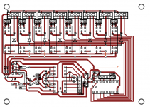
revised board layout
attached is the revised board layout that corresponds to the revised schematic. surprisingly, i was able to even make it smaller. 😎 thoughts?
p.s. it looks like the diode symbols on the board layout are backwards... silly pcb software.
thanks,
~ brad.
attached is the revised board layout that corresponds to the revised schematic. surprisingly, i was able to even make it smaller. 😎 thoughts?
p.s. it looks like the diode symbols on the board layout are backwards... silly pcb software.
thanks,
~ brad.
Attachments
You can make all the traces to the relays shorter by turning U1 90 degrees
anti-clockwise, so it is parallel to U4.
anti-clockwise, so it is parallel to U4.
#16 is a very good post, especially for all the 3-resistor-amp builders.
Yes.geekysuavo said:will the capacitance and the input impedance of the opamp form a high-pass rolloff
That depends on the capacitor you choose. f = 1 / (2*pi*R*C)geekysuavo said:at some insanely low frequency
How should we know? 😀geekysuavo said:am i smoking too much?
Hi,
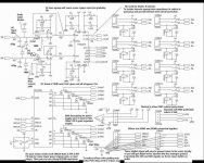
Still a few things I would recomend changing. I have done a modified CCT diagram as it much easier to understand.
I have tried to anotate it so you know what each thing does and you can decide if you want to implement it or not.
Hopefully the attached image will work; it was modified in paint so is a bit messy, then I had to compress the JPG alot to get it under the file limit.
Regards,
Andrew
Attachments
wow, this is a great help Andrew! i'll definitely work in the HF and LF filters to the inputs of the opamp.
i know the relays will draw significant current, but i'm kind of stuck with them...
actually, where should AGND and DGND connect together? i know i'll have separate power and signal star grounds, but should there even be a separate digital star ground as well? then all three would connect at the final star...
speaking of grounds, i'll also isolate the left and right grounds to reduce crosstalk.
you'll have to excuse my lack of knowledge on this, but what effect does putting catch diodes on the buffer inputs have? also, even if there is only going to be a short (few inches long) wire connecting the preamp out to the poweramp in, are the 100R resistors necessary to isolate the pga outputs?
thanks for all the fantastic help on this!
~ brad.
The catch diodes are to prevent static voltage strikes from damaging the opamp. If the voltage on the input goes above or below the rail voltages then the diode redirects it to the power rail where it will be smoothed out by the bulk storage capacitors.
I would still recomend the 100R resistors as if you short the output when connecting the amplifier it will prevent damage to the PGA, also if there is some parasitic capacitance to GND on either PCB it could cause instability (although this is very unlikley).
The classic place to connect AGND and DGND would be at the PGA since it is connected to both. If I remeber correctly they are joined together inside the chip, (you could check this with a multimeter) so if they are at different potentials current flows though the gound bond wires on the chip (this is not good and could cuase damage to the chip if high enough). However you need to be sure that the high currents from the relays are not flowing in this path as that could cause noise, so a seperate ground path for the digital components and the relays may be required back to the gnd on the connector to the PSU.
I guess you have already bought the relays. Might be worth considering keeping them for something else as if they are high power relays they will have a quite high contact resistance and a higher voltage / current requirement to overcome the contact oxidisation. A typical signal relay would have a requirement of -minimum permissible load: 0.01 mA 10 mVDC (example an OMRON G5A part) which you would normally see in audio. However a high power relay may require many times this to overcome the oxidisation on the contacts so you may get some distortion in low level music after the contacts close. Unfortunately power realys don't often have this requirement specified as they assume you will be switch higher voltages and currents (other wise why would you have chosen a power relay). As an example a power Omron G4W part is specified at 100mA for its reference tests indicating that they don't guarantee it below this current. Normally when new they will work at much much lower currents but as they get old and oxidise they will get noisy and cause distortion becuse the current and voltage level will not be enough to break through the oxide layer.
You probably didn't want to know that; but I did warn you that this audio stuff was actually much more complicated than most people realise. Your relays will work ok so don't think this means they are unusable, its just they are probably not optimal.
This is one of the reasons most audio companies have gone over to solid state switches because a good relay solution is expensive and a good solid state solution can be much cheaper and more reliable. The last Hi End design I was involved in we used a hermetically sealed reed relay so that the contacts wouldn't oxidise, but these are about £5 each in production volumes. The old mercury wetted types were ideal for this but you can't get these easly any more as if they break they obviously release mercury.
If you want to change to a solid sate design let me know I can give you some advice on this. The parts are cheaper but the circuit is a bit more complex if you are going to minimise errors from the CMOS switch resistance which is non linear with voltage.
Regards,
Andrew
eek! 
ok. i'll bite the bullet and buy some of the OMRON G5A-237P-DC5 type, since they're actually cheaper than the ones currently in the design and since i can drive them with a simple ULN2803.
this is a completely n00bish question, but - for the G5A - which contacts of the DPDT are NC and which are NO during zero coil voltage? my guess is 6,7 are NC?
thanks,
~ brad.
Data sheets are normal drawn showing the unenergised state. The Omron data sheet I found showed the contacts in the 5 / 8 position, so I would expect this to be the NC contacts with no power on the coil.
Regards,
Andrew
Regards,
Andrew
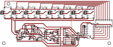
the yet again revised schematic
ok, i've made revisions based on the following recommendations:
* lower power (25mA) OMRON relays
* flyback diodes on the opamp inputs
* HP and LP filters on the opamp inputs
* 100R resistors at PGA outputs
* separate right and left channel grounds
this input has absolutely been extremely helpful so far. i'm learning alot! 🙂
~ brad.
P.S. the 47pF caps should actually be 470pF, for a rolloff at 33.86kHz.
Attachments
The recommended roll-off for audio amplifiers is between 100 kHz and 300 kHz. That is because the frequency at which a filter starts to have an audible influence is ~5 times from its corner frequency.
Hi,
I noticed that R6 is the wrong side of the AC coupling cap C14.
I had put 100R resistors with 470p as an HF filter (I realise the diagram was very difficult to read). You could certainly bring this down quite alot if you want tighter filtering. However as pointed out in the previous email you don't really want to go down to a 33KHz 3dB point as you will have some fairly significant amplitude effects at 20KHz and significant phase effects.
You still need some form of ground going back to the microcontroller with the digital signals. Even if you don't have a seperate one for the clocks, you do need a defined ground return otherwise you will get signal intergity problems. So you need to add at least one ground return to each of the connectors. Otherwise the loop area between the return path, which would presumably be through the PSU, will be very large. This will cause signal itegrity problems and crosstalk problems. (Not to mention EMC problems, which could be a problem if you interfere with next doors TV or radio)
LGND and RGND need to be joined together, I often do this with a 0R resistor as you can then put a few options on and see which one works best, and it stops you running into problems with the layout package. Once these are connected together you will also need a conection to DGND; again a 0R resistor could be used.
I am holding myself back from a long lecture on schematic style as its not really a problem in a home build. I bet your really gald your not part of my design team 🙂
Regards,
Andrew
pacificblue said:The recommended roll-off for audio amplifiers is between 100 kHz and 300 kHz. That is because the frequency at which a filter starts to have an audible influence is ~5 times from its corner frequency.
wow, good info. 🙂 fixed in the current schematic.
gfiandy said:I noticed that R6 is the wrong side of the AC coupling cap C14.
fixed in the schematic, which i know is not as clean as one would like. the board reflects this change.
gfiandy said:I had put 100R resistors with 470p as an HF filter (I realise the diagram was very difficult to read). You could certainly bring this down quite alot if you want tighter filtering. However as pointed out in the previous email you don't really want to go down to a 33KHz 3dB point as you will have some fairly significant amplitude effects at 20KHz and significant phase effects.
i tightened the HF -3dB point to 340 kHz.
gfiandy said:You still need some form of ground going back to the microcontroller with the digital signals.
i'm not sure i follow. there is a digital ground, separate from the analog grounds.
gfiandy said:LGND and RGND need to be joined together, I often do this with a 0R resistor as you can then put a few options on and see which one works best, and it stops you running into problems with the layout package. Once these are connected together you will also need a conection to DGND; again a 0R resistor could be used.
all the grounds will connect together at a final star connection point in the chassis.
gfiandy said:I am holding myself back from a long lecture on schematic style as its not really a problem in a home build.
thanks. 🙂 honestly, at this point, i really just want to know if the board will perform well enough for everyday use. i'm not looking to release a groundbreaking design, just something that sounds good and works well when i listen to my music.
gfiandy said:I bet your really gald your not part of my design team 🙂
actually, your insights have forced me to understand every part of the schematic at more depth than i did originally. you've helped alot.
thanks,
~ brad.
Attachments
Hi,
At high frequency the signal flows in the electric field between the outgoing signal wire and the return ground wire.
So if the return ground is via a star point on the chassis of the unit the digital signals will all be flowing in a field between the outgoing signal wire and the return path through the star earth. This will cause crosstalk between the signals and because there will be alot of inductance in the return path ringing on the signals.
Practical upshot of this for reliable operation you need a ground return from the preamp PCB to the digital PCB on the same conector as the digital signals. So the signal can go out on one wire and return on the other.
For really high speed operation it is normal to make every other wire a ground return so each signal has its own ground wire next to it. For your design this isn't necessary, and in fact it will probably work even if you don't have the ground returns depending on how fast you run the clocks to the two chips. However the electric field will interact with the analogue parts and probably degrade the sound.
In high frequency work a ground plane is used (litteraly a sheet of meal on another layer of the PCB) so that the signals can return as close as possible to the outgoing track. At high frequency the return current will literally go back underneath the track that it went out on a ground plane, even though it could use the whole plane, the reduction in the inductance if it flows close to the outgoing signal makes this the "path of least resistance")
Finally indiscriminant use of a star earth will not work, it is not a panacea for ground problems you need to think about where the currents flow and work out the best configuration. Often this is not a star. Sometimes it is better to use a ground follows signal topology or a combination of star grounding on each PCB with ground follows signal between PCBs. Or in some system a star of stars is the most appropriate way to work.
You need to establish were grounds are connected together inside components as this will dictate some of the ground connections.
Also think about where the signal comes from, electrical circuits work in loops. There is no real ground (in fact the whole concept is very misleading) in a product the signals all flow in loops from a power source (often the decoupling capacitors on a chip) through something controlling the power (OPAMPs in this case) to the load (the power amplifer input in this case) and back from the ground end of the load via the ground structure back to the power source and this last part is just as mcuh part of the circuit as the outgoing path.
So the left and right signals will flow from the opamps down thier seperate wires to the power amplifer go into the input of the power amplifer then the signal will flow out of the input stage of the amplifer and find its way back to the power supply on the opamp via the left and right ground returns.
Practical upshot in this situation. You need to conect the L and R grounds together on the preamplifer PCB as they are connected together inside the PGA chip and if you connect them at the star and at the PGA chip you will have a ground loop that will probably pick up hum. The same is ture for DGND and (LGND + RGND); DGND is connected to LGND and RGND inside the PGA chip so if you connect them back at the PSU as well you will have created a ground loop.
Connecting one rail on the PGA to LGND -ve12 and one to RGND +12ve means that the signals will have an asymetric return path. i.e the right signal can return easly to the positive rail but has to go via the internal ground path inside the chip to get to the -ve rail (or via the star if you had connected that as well) and visa versa. This will cause problems probably distrotion and instability.
Basically it would have been better to stay with one wire than split the grounds the way you have now. I only suggested seperate grounds for left and right to reduce the interaction between left and right on the resistance of the ground wire between the pre aplifer and the power amplifer.
Sorry I have rambled a bit here. If its not clear let me know and I will try to explain it better. Unfortunately grounding is complex and requires carefull consideration of many competing requirements that need a compromise to be drawn between them.
Regards,
Andrew
eep!
wow. ok. well... so as the circuit is, the best improvement would be to connect all grounds together on the board and send the final ground out through a single wire?
thanks,
~ brad.
wow. ok. well... so as the circuit is, the best improvement would be to connect all grounds together on the board and send the final ground out through a single wire?
thanks,
~ brad.
I can't answer this question simply.
You need to know how all the other bits are going to be powered and what signals need to go between the boards.
For example will both the power amplifer and the preamplifer be connected to the micro controller. If so you could easly end up with a ground loop through the preamplifer ground over to the power amplifer and back from the power amplifer to the microcontroller.
You also need to know where power supplies are shared between different PCBs and where they are completely seperate and float from each other.
With this information you can make a guess at the best topology.
What I can tell you is that the signals gnds that are all connected to the PGA all need to connect together on the preamplifer PCB.
Regards,
Andrew
alright, sounds like i've got a bit of contemplation to do for finalizing this design. thanks for all of the help in nudging me towards the right direction. 🙂
~ brad.
~ brad.
- Status
- Not open for further replies.
- Home
- Amplifiers
- Chip Amps
- PGA2310 and Source Selection, right direction?